MAX3421EEHJ+T Maxim Integrated Products, MAX3421EEHJ+T Datasheet - Page 19

MAX3421EEHJ+T
Manufacturer Part Number
MAX3421EEHJ+T
Description
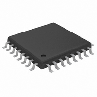
IC USB PERIPH/HOST CNTRL 32TQFP
Manufacturer
Maxim Integrated Products
Datasheet
1.MAX3421EETJ.pdf
(32 pages)
Specifications of MAX3421EEHJ+T
Controller Type
USB Peripheral Controller
Interface
USB/Serial
Voltage - Supply
3 V ~ 3.6 V
Current - Supply
15mA
Operating Temperature
-40°C ~ 85°C
Mounting Type
Surface Mount
Package / Case
32-TQFP, 32-VQFP
For Use With
MAX3421EVKIT-1+ - EVAL KIT FOR MAX3421E
Lead Free Status / RoHS Status
Lead free / RoHS Compliant
• INIRQ: When the SEPIRQ bit of the MODE
• SOF: A square wave with a positive edge that
The SPI data pins MOSI and MISO operate differently
depending on the setting of a register bit called FDUPSPI
(full-duplex SPI). Figure 15 shows the two configurations
according to the FDUPSPI bit setting.
In full-duplex mode (FDUPSPI = 1), the MOSI and MISO
pins are separate, and the MISO pin drives only when SS
is low. In this mode, the first eight SCLK edges (after SS =
0) clock the command byte into the MAX3421E on MOSI,
and 8 USB status bits are clocked out of the MAX3421E
on MISO. For an SPI write cycle, any bytes following the
command byte are clocked into the MAX3421E on MOSI,
and zeros are clocked out on MISO. For an SPI read
cycle, any bytes following the command byte are clocked
out of the MAX3421E on MISO and the data on MOSI is
ignored. At the conclusion of the SPI cycle (SS = 1), the
MISO output tri-states.
In half-duplex mode, the MOSI pin is a bidirectional pin
and the MISO pin is tri-stated. This saves a pin in the SPI
interface. Because of the shared data pin, this mode
does not offer the 8 USB status bits (Figures 6 and 7) as
Figure 16. SPI Clocking Modes
(R27) register is set high, the BUSACT signal is
removed from the INT output and GPX is used as
an IRQ output pin dedicated to GPIN interrupts if
GPX[B:A] = 10. In this mode, GPIN interrupts
appear only on the GPX pin, and do not appear on
the INT output pin.
indicates the USB start-of-frame (Figure 14).
MODE 0,0
MODE 1,1
MISO
SCLK
SCLK
MOSI
SS
MOSI (Master-Out, Slave-In) and
______________________________________________________________________________________
MISO (Master-In, Slave-Out)
D7
Q7
D6
Q6
USB Peripheral/Host Controller
D5
Q5
*MSB OF NEXT BYTE IN BURST MODE (SS REMAINS LOW)
D4
Q4
SPI MODE 0,0 OR 1,1
the command byte is clocked into the MAX3421E. The
MISO pin can be left unconnected in half-duplex mode.
The SPI master provides the MAX3421E SCLK signal to
clock the SPI interface. SCLK has no low-frequency limit,
and can be as high as 26MHz. The MAX3421E changes
its output data (MISO) on the falling edge of SCLK and
samples input data (MOSI) on the rising edge of SCLK.
The MAX3421E ignores SCLK transitions when SS is
high. The inactive level of SCLK may be low or high,
depending on the SPI operating mode (Figure 16).
The MAX3421E SPI interface is active only when SS is
low. When SS is high, the MAX3421E tri-states the SPI
output pin and resets the internal MAX3421E SPI logic.
If SS goes high before a complete byte is clocked in,
the byte-in-progress is discarded. The SPI master can
terminate an SPI cycle after clocking in the first 8 bits
(the command byte). This feature can be used in a full-
duplex system to retrieve the USB status bits (Figure 6
and 7) without sending or receiving SPI data.
The MAX3421E operates as an SPI slave device. A reg-
ister access consists of the SPI master first writing an
SPI command byte, followed by reading or writing the
contents of the addressed register (see the Register
Description section for more details). All SPI transfers
are MSB first. The external SPI master provides a clock
signal to the MAX3421E SCLK input. This clock fre-
quency can be between DC and 26MHz. Bit transfers
D3
Q3
D2
Q2
with SPI Interface
Applications Information
D1
Q1
D0
Q0
SCLK (Serial Clock)
SS (Slave Select)
*
SPI Interface
*
19


