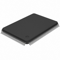
DS21Q41BT Maxim Integrated Products, DS21Q41BT Datasheet - Page 33

DS21Q41BT
Manufacturer Part Number
DS21Q41BT
Description
IC FRAMER T1 QUAD 128-TQFP
Manufacturer
Maxim Integrated Products
Datasheet
1.DS21Q41BT.pdf
(61 pages)
Specifications of DS21Q41BT
Controller Type
T1 Framer
Interface
Parallel/Serial
Voltage - Supply
4.5 V ~ 5.5 V
Current - Supply
30mA
Operating Temperature
0°C ~ 70°C
Mounting Type
Surface Mount
Package / Case
128-TQFP, 128-VQFP
Lead Free Status / RoHS Status
Contains lead / RoHS non-compliant
Available stocks
Company
Part Number
Manufacturer
Quantity
Price
Company:
Part Number:
DS21Q41BT
Manufacturer:
DS
Quantity:
3 279
Part Number:
DS21Q41BT
Manufacturer:
MAXIM/美信
Quantity:
20 000
Company:
Part Number:
DS21Q41BTN
Manufacturer:
DALLAS
Quantity:
104
The DS21Q41B also contains a 0 destuffer which is controlled via the CCR2.0 bit. In both ANSI T1.403
and TR54016, communications on the FDL follows a subset of a LAPD protocol. The LAPD protocol
states that no more than five 1s should be transmitted in a row so that the data does not resemble an
opening or closing flag (01111110) or an abort signal (11111111). If enabled via CCR2.0, the DS21Q41B
will automatically look for five 1s in a row, followed by a 0. If it finds such a pattern, it will automatically
remove the 0. If the 0 destuffer sees six or more 1s in a row followed by a 0, the 0 is not removed. The
CCR2.0 bit should always be set to a 1 when the DS21Q41B is extracting the FDL. More on how to use
the DS21Q41B in FDL applications is covered in a separate Application Note.
RFDL: RECEIVE FDL REGISTER (Address=28 Hex)
The Receive FDL Register (RFDL) reports the incoming Facility Data Link (FDL) or the incoming Fs
bits. The LSB is received first.
RFDLM1: RECEIVE FDL MATCH REGISTER 1 (Address=29 Hex)
RFDLM2: RECEIVE FDL MATCH REGISTER 2 (Address=2A Hex)
When the byte in the Receive FDL Register matches either of the two Receive FDL Match Registers
(RFDLM1/RFDLM2), RSR2.2 will be set to a 1 and the
6.2 Transmit Section
The transmit section will shift out into the T1 data stream, either the FDL (in the ESF framing mode) or
the Fs bits (in the D4 framing mode) contained in the Transmit FDL register (TFDL). When a new value
is written to the TFDL, it will be multiplexed serially (LSB first) into the proper position in the outgoing
T1 data stream. After the full 8 bits have been shifted out, the DS21Q41B will signal the host
microcontroller that the buffer is empty and that more data is needed by setting the SR2.3 bit to a 1. The
update the TFDL with a new value. If the TFDL is not updated, the old value in the TFDL will be
transmitted once again.
The DS21Q41B also contains a 0 stuffer which is controlled via the CCR2.4 bit. In both ANSI T1.403
and TR54016, communications on the FDL follows a subset of a LAPD protocol. The LAPD protocol
INT
(MSB)
(MSB)
RFDL7
RFDL7
will also toggle low if enabled via IMR2.3. The user has 2 ms (1.5 ms in SLC-96 applications) to
SYMBOL
SYMBOL
RFDL7
RFDL0
RFDL7
RFDL0
RFDL6
RFDL6
POSITION
POSITION
RFDL.7
RFDL.0
RFDL.7
RFDL.0
RFDL5
RFDL5
NAME AND DESCRIPTION
MSB of the received FDL code
LSB of the received FDL code
NAME AND DESCRIPTION
MSB of the FDL match code
LSB of the FDL match code
RFDL4
RFDL4
33 of 61
RFDL3
RFDL3
INT
will go active if enabled via IMR2.2.
RFDL2
RFDL2
RFDL1
RFDL1
RFDL0
RFDL0
DS21Q41B
(LSB)
(LSB)


