DS31412 Maxim Integrated Products, DS31412 Datasheet - Page 22
DS31412
Manufacturer Part Number
DS31412
Description
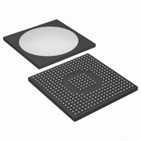
IC 12CH DS3/3 FRAMER 349-BGA
Manufacturer
Maxim Integrated Products
Datasheet
1.DS3148.pdf
(89 pages)
Specifications of DS31412
Controller Type
DS3/E3 Framer
Interface
LIU
Voltage - Supply
3.135 V ~ 3.465 V
Current - Supply
960mA
Operating Temperature
-40°C ~ 85°C
Mounting Type
Surface Mount
Package / Case
349-BGA
Lead Free Status / RoHS Status
Lead free / RoHS Compliant
Available stocks
Company
Part Number
Manufacturer
Quantity
Price


7.6 Common and Line Interface Registers
This section describes the registers responsible for top-level configuration, control, and status of each framer,
including resets, clocks, pin controls, and line interface functions.
Table 7-C. Common Line Interface Register Map
Register Name:
Register Description:
Register Address:
Bit #
Name
Default
This register is a global resource and is mapped into address 00h in every framer in the device.
Bits 0 to 7: Device ID (ID[7:0]). Read-only. Contact the factory for details on the meaning of the ID bits.
Register Name:
Register Description:
Register Address:
Bit #
Name
Default
Bit 0: Framer Reset (RST). When this bit is set to logic 1, it forces all of the internal registers in the framer (except
this RST bit) to their default state. Only the framer associated with this register is reset. RST must be high for a
minimum of 100ns and then returned low. This register bit is logically ORed with the RST pin.
Bit 1: Framer Disable (DISABLE). Setting this bit disables the framer by stopping all clocks. This reduces the
power the framer requires. After the framer is enabled again by clearing this bit, the RST bit must be toggled to
initialize the framer again. Toggling the RST bit when DISABLE = 1 automatically enables the framer again.
Bit 2: Transmit Unframed All Ones (TUA1). Enables the transmission of an unframed all-ones pattern on
TPOS/TNEG or TNRZ. This pattern is sometimes called physical AIS.
ADDR
0Ah
00h
01h
02h
03h
04h
05h
06h
07h
08h
09h
0 = normal operation
1 = force all internal registers to their default values
0 = enable framer
1 = disable framer
0 = disable transmission of unframed all ones
1 = enable transmission of unframed all ones (reset default value)
REGISTER
LOTCMC
MSRIE
MSRL
ISR1
ISR2
MSR
MC1
MC2
MC3
MC4
MC5
ID7
ID
—
7
7
0
TDENMS
RDENMS
LOTCMC
LORCIE
OSTCS
LORCL
RNEGI
LORC
BIT 7
INT8
N/A
ID6
ZCSD
ID7
—
6
6
0
ID
ID Register
00h
MC1
Master Configuration Register 1
01h
LOTCIE
TCCLK
TSOFC
ROOFI
RPOSI
LOTCL
ZCSD
LOTC
BIT 6
INT7
ID6
N/A
ID5
—
BIN
5
0
5
TOHENI
T3E3IE
RLOSI
RCLKI
BIT 5
T3E3
INT6
BIN
N/A
N/A
N/A
ID5
MECU
22 of 89
ID4
—
4
4
0
TNEGH
FEACIE
RDATH
MECU
FEAC
RZSF
BIT 4
TOHI
INT5
N/A
N/A
ID4
AECU
ID3
—
3
3
0
HDLCIE
TPOSH
RSOFI
TSOFI
AECU
INT12
HDLC
BIT 3
INT4
N/A
ID3
N/A
TUA1
2
1
ID2
—
2
ROCLKI
BERTIE
TICLKI
TNEGI
INT11
BERT
BIT 2
TUA1
INT3
DLB
N/A
ID2
DISABLE
1
0
ID1
—
DISABLE
COVFIE
1
COVFL
RDATI
TPOSI
TDATI
COVF
INT10
BIT 1
INT2
LLB
ID1
RST
ID0
—
RDENI
0
0
TDENI
OSTIE
TCLKI
0
OSTL
BIT 0
INT1
INT9
RST
PLB
N/A
ID0
Related parts for DS31412
Image
Part Number
Description
Manufacturer
Datasheet
Request
R

Part Number:
Description:
MAX7528KCWPMaxim Integrated Products [CMOS Dual 8-Bit Buffered Multiplying DACs]
Manufacturer:
Maxim Integrated Products
Datasheet:
Part Number:
Description:
Single +5V, fully integrated, 1.25Gbps laser diode driver.
Manufacturer:
Maxim Integrated Products
Datasheet:
Part Number:
Description:
Single +5V, fully integrated, 155Mbps laser diode driver.
Manufacturer:
Maxim Integrated Products
Datasheet:
Part Number:
Description:
VRD11/VRD10, K8 Rev F 2/3/4-Phase PWM Controllers with Integrated Dual MOSFET Drivers
Manufacturer:
Maxim Integrated Products
Datasheet:
Part Number:
Description:
Highly Integrated Level 2 SMBus Battery Chargers
Manufacturer:
Maxim Integrated Products
Datasheet:
Part Number:
Description:
Current Monitor and Accumulator with Integrated Sense Resistor; ; Temperature Range: -40°C to +85°C
Manufacturer:
Maxim Integrated Products
Part Number:
Description:
TSSOP 14/A�/RS-485 Transceivers with Integrated 100O/120O Termination Resis
Manufacturer:
Maxim Integrated Products
Part Number:
Description:
TSSOP 14/A�/RS-485 Transceivers with Integrated 100O/120O Termination Resis
Manufacturer:
Maxim Integrated Products
Part Number:
Description:
QFN 16/A�/AC-DC and DC-DC Peak-Current-Mode Converters with Integrated Step
Manufacturer:
Maxim Integrated Products
Part Number:
Description:
TDFN/A/65V, 1A, 600KHZ, SYNCHRONOUS STEP-DOWN REGULATOR WITH INTEGRATED SWI
Manufacturer:
Maxim Integrated Products
Part Number:
Description:
Integrated Temperature Controller f
Manufacturer:
Maxim Integrated Products
Part Number:
Description:
SOT23-6/I�/45MHz to 650MHz, Integrated IF VCOs with Differential Output
Manufacturer:
Maxim Integrated Products
Part Number:
Description:
SOT23-6/I�/45MHz to 650MHz, Integrated IF VCOs with Differential Output
Manufacturer:
Maxim Integrated Products
Part Number:
Description:
EVALUATION KIT/2.4GHZ TO 2.5GHZ 802.11G/B RF TRANSCEIVER WITH INTEGRATED PA
Manufacturer:
Maxim Integrated Products
Part Number:
Description:
QFN/E/DUAL PCIE/SATA HIGH SPEED SWITCH WITH INTEGRATED BIAS RESISTOR
Manufacturer:
Maxim Integrated Products
Datasheet: