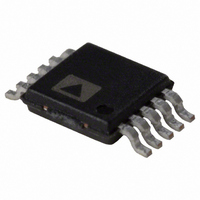
AD9833BRMZ Analog Devices Inc, AD9833BRMZ Datasheet

AD9833BRMZ
Specifications of AD9833BRMZ
Available stocks
Related parts for AD9833BRMZ
AD9833BRMZ Summary of contents
Page 1
FEATURES Digitally programmable frequency and phase 12.65 mW power consumption MHz to 12.5 MHz output frequency range 28-bit resolution: 0 MHz reference clock Sinusoidal, triangular, and square wave outputs 2 5.5 ...
Page 2
AD9833 TABLE OF CONTENTS Features .............................................................................................. 1 Applications ....................................................................................... 1 General Description ......................................................................... 1 Functional Block Diagram .............................................................. 1 Revision History ............................................................................... 2 Specifications ..................................................................................... 3 Timing Characteristics ................................................................ 4 Absolute Maximum Ratings ............................................................ 5 ESD Caution .................................................................................. 5 Pin ...
Page 3
SPECIFICATIONS VDD = 2 5.5 V, AGND = DGND = Table 1. 1 Parameter SIGNAL DAC SPECIFICATIONS Resolution Update Rate VOUT Maximum VOUT Minimum VOUT Temperature Coefficient DC Accuracy Integral Nonlinearity Differential Nonlinearity DDS SPECIFICATIONS ...
Page 4
AD9833 TIMING CHARACTERISTICS VDD = 2 5.5 V, AGND = DGND = 0 V, unless otherwise noted. Table 2. Parameter Limit MIN MAX ...
Page 5
ABSOLUTE MAXIMUM RATINGS T = 25°C, unless otherwise noted. A Table 3. Parameter VDD to AGND VDD to DGND AGND to DGND CAP/2.5V Digital I/O Voltage to DGND Analog I/O Voltage to AGND Operating Temperature Range Industrial (B Version) Storage ...
Page 6
AD9833 PIN CONFIGURATION AND FUNCTION DESCRIPTIONS Table 4. Pin Function Descriptions Pin No. Mnemonic Description 1 COMP DAC Bias Pin. This pin is used for decoupling the DAC bias voltage. 2 VDD Positive Power Supply for the Analog and Digital ...
Page 7
TYPICAL PERFORMANCE CHARACTERISTICS 5 25°C A 5.0 VDD = 5V 4.5 VDD = 3V 4.0 3.5 3 MCLK FREQUENCY (MHz) Figure 6. Typical Current Consumption (I for f = MCLK/10 OUT 6 VDD = ...
Page 8
AD9833 1000 950 900 850 800 750 VDD = 5.5V 700 650 600 550 500 –40 25 TEMPERATURE (°C) Figure 12. Wake-Up Time vs. Temperature 1.250 1.225 UPPER RANGE 1.200 1.175 LOWER RANGE 1.150 1.125 1.100 –40 25 TEMPERATURE (°C) ...
Page 9
RWB 300 VWB 100 FREQUENCY (Hz) Figure 18. Power vs. Frequency MHz, f MCLK Frequency Word = 0x009D495 0 –10 –20 –30 –40 –50 –60 ...
Page 10
AD9833 TERMINOLOGY Integral Nonlinearity (INL) INL is the maximum deviation of any code from a straight line passing through the endpoints of the transfer function. The end- points of the transfer function are zero scale, a point 0.5 LSB below ...
Page 11
THEORY OF OPERATION Sine waves are typically thought of in terms of their magnitude form: a(t) = sin(ωt). However, these sine waves are nonlinear and not easy to generate except through piecewise construction. On the other hand, the angular information ...
Page 12
AD9833 CIRCUIT DESCRIPTION The AD9833 is a fully integrated direct digital synthesis (DDS) chip. The chip requires one reference clock, one low precision resistor, and decoupling capacitors to provide digitally created sine waves up to 12.5 MHz. In addition to ...
Page 13
FUNCTIONAL DESCRIPTION SERIAL INTERFACE The AD9833 has a standard 3-wire serial interface that is compatible with the SPI, QSPI™, MICROWIRE®, and DSP interface standards. Data is loaded into the device as a 16-bit word under the control of a serial ...
Page 14
AD9833 Table 6. Description of Bits in the Control Register Bit Name Function D13 B28 Two write operations are required to load a complete word into either of the frequency registers. B28 = 1 allows a complete word to be ...
Page 15
FREQUENCY AND PHASE REGISTERS The AD9833 contains two frequency registers and two phase registers, which are described in Table 7. Table 7. Frequency and Phase Registers Register Size Description FREQ0 28 bits Frequency Register 0. When the FSELECT bit = ...
Page 16
AD9833 RESET FUNCTION The reset function resets appropriate internal registers provide an analog output of midscale. Reset does not reset the phase, frequency, or control registers. When the AD9833 is powered up, the part should be reset. ...
Page 17
APPLICATIONS INFORMATION Because of the various output options available from the part, the AD9833 can be configured to suit a wide variety of applications. One of the areas where the AD9833 is suitable is in modulation applications. The part can ...
Page 18
AD9833 OUT YES CHANGE FSELECT? YES CHANGE FREQUENCY REGISTER? CONTROL REGISTER WRITE (SEE TABLE 6) DATA WRITE (SEE FIGURE 28) SELECT DATA SOURCES WAIT 7/8 MCLK CYCLES DAC OUTPUT × 18 × × (1 ...
Page 19
DATA WRITE WRITE A FULL 28-BIT WORD FREQUENCY REGISTER FREQUENCY REGISTER? YES (CONTROL REGISTER WRITE) (CONTROL REGISTER WRITE) B28 (D13 WRITE TWO CONSECUTIVE 16-BIT WORDS (SEE TABLE 10 AND TABLE 11 (SEE ...
Page 20
AD9833 INTERFACING TO MICROPROCESSORS The AD9833 has a standard serial interface that allows the part to interface directly with several microprocessors. The device uses an external serial clock to write the data or control information into the device. The serial ...
Page 21
EVALUATION BOARD The AD9833 evaluation board allows designers to evaluate the high performance AD9833 DDS modulator with a minimum of effort. SYSTEM DEMONSTRATION PLATFORM The system demonstration platform (SDP hardware and software evaluation tool for use in conjunction ...
Page 22
AD9833 EVALUATION BOARD SCHEMATICS Figure 34. Evaluation Board Schematic Figure 35. SDP Connector Schematic Rev Page ...
Page 23
EVALUATION BOARD LAYOUT Figure 36. AD9833 Evaluation Board Component Side Figure 37. AD9833 Evaluation Board Silkscreen Figure 38. AD9833 Evaluation Board Solder Side Rev Page AD9833 ...
Page 24
... AD9833BRM-REEL −40°C to +105°C AD9833BRM-REEL7 −40°C to +105°C AD9833BRMZ −40°C to +105°C AD9833BRMZ-REEL −40°C to +105°C AD9833BRMZ-REEL7 −40°C to +105°C AD9833WBRMZ-REEL −40°C to +105°C EVAL-AD9833SDZ RoHS Compliant Part Qualified for Automotive Applications. ...


