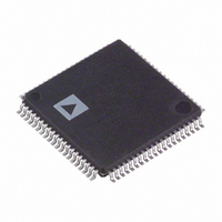
AD9852ASTZ Analog Devices Inc, AD9852ASTZ Datasheet - Page 35

AD9852ASTZ
Manufacturer Part Number
AD9852ASTZ
Description
IC DDS SYNTHESIZER CMOS 80-LQFP
Manufacturer
Analog Devices Inc
Datasheet
1.AD9852ASTZ.pdf
(52 pages)
Specifications of AD9852ASTZ
Resolution (bits)
12 b
Master Fclk
200MHz
Tuning Word Width (bits)
48 b
Voltage - Supply
3.14 V ~ 3.47 V
Operating Temperature
-40°C ~ 85°C
Mounting Type
Surface Mount
Package / Case
80-LQFP
Pll Type
Frequency Synthesis
Frequency
100MHz
Supply Current
660mA
Supply Voltage Range
3.135V To 3.465V
Digital Ic Case Style
LQFP
No. Of Pins
80
Operating Temperature Range
-40°C To +85°C
Lead Free Status / RoHS Status
Lead free / RoHS Compliant
For Use With
AD9852/PCBZ - BOARD EVAL FOR AD9852
Lead Free Status / RoHS Status
Lead free / RoHS Compliant, Lead free / RoHS Compliant
Available stocks
Company
Part Number
Manufacturer
Quantity
Price
Company:
Part Number:
AD9852ASTZ
Manufacturer:
ALTERA
Quantity:
210
Company:
Part Number:
AD9852ASTZ
Manufacturer:
Analog Devices Inc
Quantity:
135
Company:
Part Number:
AD9852ASTZ
Manufacturer:
ADI
Quantity:
260
Company:
Part Number:
AD9852ASTZ
Manufacturer:
Analog Devices Inc
Quantity:
10 000
Part Number:
AD9852ASTZ
Manufacturer:
ADI/亚德诺
Quantity:
20 000
SERIAL INTERFACE PORT PIN DESCRIPTIONS
Table 12.
Pin
SCLK
CS
SDIO
SDO
IO RESET
Notes on Serial Port Operation
The AD9852 serial port configuration bits reside in Bit 1 and Bit 0
of Register Address 20 hex. The configuration changes immediately
upon a valid I/O update. For multibyte transfers, writing to this
register can occur during the middle of a communication cycle.
Care must be taken to compensate for this new configuration
during the remainder of the current communication cycle.
The system must maintain synchronization with the AD9852;
otherwise, the internal control logic is not able to recognize further
instructions. For example, if the system sends the instruction to
write a 2-byte register and then pulses the SCLK pin for a 3-byte
register (24 additional SCLK rising edges), communication
synchronization is lost. In this case, the first 16 SCLK rising
edges after the instruction cycle properly write the first two data
bytes into the AD9852, but the subsequent eight rising SCLK
edges are interpreted as the next instruction byte, not the final
byte of the previous communication cycle.
In cases where synchronization is lost between the system and
the AD9852, the IO RESET pin provides a means to re-establish
synchronization without reinitializing the entire chip. Asserting
the IO RESET pin (active high) resets the AD9852 serial port
state machine, terminating the current I/O operation and forcing
the device into a state in which the next eight SCLK rising edges
are understood to be an instruction byte. The IO RESET pin
must be deasserted (low) before the next instruction byte write
can begin. Any information written to the AD9852 registers
during a valid communication cycle prior to loss of synchro-
nization remains intact.
Description
Serial Clock (Pin 21). The serial clock pin is used to synchronize data to and from the AD9852 and to run the internal state
machines. The SCLK maximum frequency is 10 MHz.
Chip Select (Pin 22). Active low input that allows more than one device on the same serial communication line. The SDO and
SDIO pins go to a high impedance state when this input is high. If this pin is driven high during a communication cycle, the
cycle is suspended until CS is reactivated low. The chip select pin can be tied low in systems that maintain control of SCLK.
Serial Data I/O (Pin 19). Data is always written to the AD9852 on this pin. However, this pin can be used as a bidirectional data
line. The configuration of this pin is controlled by Bit 0 of Register Address 20 hex. The default is Logic 0, which configures the
SDIO pin as bidirectional.
Serial Data Out (Pin 18). Data is read from this pin for protocols that use separate lines for transmitting and receiving data.
In the case where the AD9852 operates in a single bidirectional I/O mode, this pin does not output data and is set to a high
impedance state.
Synchronize I/O Port (Pin 17). Synchronizes the I/O port state machines without affecting the contents of the addressable
registers. An active high input on the IO RESET pin causes the current communication cycle to terminate. After the IO RESET pin
returns low (Logic 0), another communication cycle can begin, starting with the instruction byte.
Rev. E | Page 35 of 52
MSB/LSB TRANSFERS
The AD9852 serial port can support both MSB- and LSB-first
data formats. This functionality is controlled by Bit 1 of Serial
Bank 20 hex. When this bit is set active high, the AD9852 serial
port is in LSB-first format. This bit defaults low, to the MSB-first
format. The instruction byte must be written in the format
indicated by Bit 1 of Serial Register Bank 20 hex. Therefore, if
the AD9852 is in LSB-first mode, the instruction byte must be
written from LSB to MSB.
SCLK
SDIO
SCLK
SDIO
SDO
CS
CS
SYMBOL
t
t
t
t
t
t
PRE
SCLK
DSU
SCLKPWH
SCLKPWL
DHLD
Figure 53. Timing Diagram for Data Write to AD9852
Figure 54. Timing Diagram for Read from AD9852
t
t
PRE
DSU
FIRST BIT
SYMBOL
t
DV
t
SCLKPWH
MIN
30ns
100ns
30ns
40ns
40ns
0ns
FIRST BIT
t
DHLD
t
SCLK
DEFINITION
CS SETUP TIME
PERIOD OF SERIAL DATA CLOCK
SERIAL DATA SETUP TIME
SERIAL DATA CLOCK PULSE WIDTH HIGH
SERIAL DATA CLOCK PULSE WIDTH LOW
SERIAL DATA HOLD TIME
MAX
30ns
t
SCLKPWL
t
DV
DEFINITION
DATA VALID TIME
SECOND BIT
SECOND BIT
AD9852


