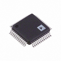
AD9859YSVZ Analog Devices Inc, AD9859YSVZ Datasheet - Page 7

AD9859YSVZ
Manufacturer Part Number
AD9859YSVZ
Description
IC DDS DAC 10BIT 400MSPS 48-TQFP
Manufacturer
Analog Devices Inc
Datasheet
1.AD9859YSVZ-REEL7.pdf
(24 pages)
Specifications of AD9859YSVZ
Resolution (bits)
10 b
Master Fclk
400MHz
Tuning Word Width (bits)
32 b
Voltage - Supply
1.71 V ~ 1.96 V
Operating Temperature
-40°C ~ 105°C
Mounting Type
Surface Mount
Package / Case
48-TQFP Exposed Pad, 48-eTQFP, 48-HTQFP, 48-VQFP
Data Rate
25Mbps
Rf Ic Case Style
TQFP
No. Of Pins
48
Supply Voltage Range
1.71V To 1.89V, 3.135V To 3.465V
Operating Temperature Range
-40°C To +105°C
Msl
MSL 3 - 168 Hours
Frequency Max
400MHz
Lead Free Status / RoHS Status
Lead free / RoHS Compliant
For Use With
AD9859/PCB - BOARD EVAL FOR AD9859
Lead Free Status / Rohs Status
Compliant
Available stocks
Company
Part Number
Manufacturer
Quantity
Price
Company:
Part Number:
AD9859YSVZ
Manufacturer:
Analog Devices Inc
Quantity:
10 000
Company:
Part Number:
AD9859YSVZ-REEL7
Manufacturer:
Analog Devices Inc
Quantity:
10 000
PIN FUNCTION DESCRIPTIONS
Table 3. Pin Function Descriptions—48-Lead TQFP/EP
Pin No.
1
2, 34
3, 33, 42, 47,
48
4, 6, 13, 16, 18,
19, 25, 27, 29
5, 7, 14, 15, 17,
22, 26, 28, 30,
31, 32
8
9
10
11
12
20
21
23
24
35
36
37
38
39
40
41
43
44
45
46
<49>
Mnemonic
I/O UPDATE
DVDD
DGND
AVDD
AGND
OSC/
OSC/REFCLK
CRYSTAL OUT
CLKMODESELECT
LOOP_FILTER
IOUT
IOUT
DACBP
DAC_R
PWRDWNCTL
RESET
IOSYNC
SDO
CS
SCLK
SDIO
DVDD_I/O
SYNC_IN
SYNC_CLK
OSK
AGND
REFCLK
SET
I/O
I
I
I
I
I
I
I
O
I
I
O
O
I
I
I
I
I
O
I
I
I/O
I
I
O
I
I
Description
The rising edge transfers the contents of the internal buffer memory to the I/O registers. This
pin must be set up and held around the SYNC_CLK output signal.
Digital Power Supply Pins (1.8 V).
Digital Power Ground Pins.
Analog Power Supply Pins (1.8 V).
Analog Power Ground Pins.
Complementary Reference Clock/Oscillator Input. When the REFCLK port is operated in single-
ended mode, REFCLKB should be decoupled to AVDD with a 0.1 µF capacitor.
Reference Clock/Oscillator Input. See the Clock Input section for details on the
OSCILLATOR/REFCLK operation.
Output of the Oscillator Section.
Control Pin for the Oscillator Section. When high, the oscillator section is enabled. When low,
the oscillator section is bypassed.
This pin provides the connection for the external zero compensation network of the REFCLK
multiplier’s PLL loop filter. The network consists of a 1 k Ω resistor in series with a 0.1 µF
capacitor tied to AVDD.
Complementary DAC Output. Should be biased through a resistor to AVDD, not AGND.
DAC Output. Should be biased through a resistor to AVDD, not AGND.
DAC Band Gap Decoupling Pin. A 0.1 μF capacitor to AGND is recommended.
A resistor (3.92 kΩ nominal) connected from AGND to DAC_R
current for the DAC.
Input Pin Used as an External Power-Down Control (see Table 8 for details).
Active High Hardware Reset Pin. Asserting the RESET pin forces the AD9859 to the initial state,
as described in the I/O port register map.
Asynchronous Active High Reset of the Serial Port Controller. When high, the current I/O
operation is immediately terminated, enabling a new I/O operation to commence once IOSYNC
is returned low. If unused, ground this pin; do not allow this pin to float.
When operating the I/O port as a 3-wire serial port, this pin serves as the serial data output.
When operated as a 2-wire serial port, this pin is unused and can be left unconnected.
This pin functions as an active low chip select that allows multiple devices to share the I/O bus.
This pin functions as the serial data clock for I/O operations.
When operating the I/O port as a 3-wire serial port, this pin serves as the serial data input only.
When operated as a 2-wire serial port, this pin is the bidirectional serial data pin.
Digital Power Supply (for I/O Cells Only, 3.3 V).
Input Signal Used to Synchronize Multiple AD9859s. This input is connected to the SYNC_CLK
output of a master AD9859.
Clock Output Pin Serves as a Synchronizer for External Hardware.
Input Pin Used to Control the Direction of the Shaped On-Off Keying Function when
Programmed for Operation. OSK is synchronous to the SYNC_CLK pin. When OSK is not
programmed, this pin should be tied to DGND.
The exposed paddle on the bottom of the package is a ground connection for the DAC and
must be attached to AGND in any board layout.
Rev. A | Page 7 of 24
SET
establishes the reference
AD9859


