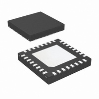
DS91M040TSQ/NOPB National Semiconductor, DS91M040TSQ/NOPB Datasheet - Page 3

DS91M040TSQ/NOPB
Manufacturer Part Number
DS91M040TSQ/NOPB
Description
IC TRANSCEIVER M-LVDS QUAD 32LLP
Manufacturer
National Semiconductor
Type
Transceiverr
Datasheet
1.DS91M040TSQNOPB.pdf
(16 pages)
Specifications of DS91M040TSQ/NOPB
Number Of Drivers/receivers
4/4
Protocol
LVDS
Voltage - Supply
3 V ~ 3.6 V
Mounting Type
Surface Mount
Package / Case
32-LLP
Device Type
Transceiver
Supply Current Max
67mA
Signaling Rate
250Mbps
Output Level Type
LVCMOS
Supply Voltage Range
3V To 3.6V
Esd Hbm
8kV
Operating Temperature Range
-40°C To +85°C
Rohs Compliant
Yes
For Use With
DS91M040EVK - BOARD EVALUATION DS91M040
Lead Free Status / RoHS Status
Lead free / RoHS Compliant
Other names
DS91M040TSQTR
Available stocks
Company
Part Number
Manufacturer
Quantity
Price
Company:
Part Number:
DS91M040TSQ/NOPB
Manufacturer:
TI
Quantity:
1 710
Part Number:
DS91M040TSQ/NOPB
Manufacturer:
TI/德州仪器
Quantity:
20 000
Pin Descriptions
M-LVDS Receiver Types
The EIA/TIA-899 M-LVDS standard specifies two different
types of receiver input stages. A type 1 receiver has a con-
ventional threshold that is centered at the midpoint of the input
amplitude, V
100mV greater then V
a failsafe circuit where open or short circuits at the input will
always result in the output stage being driven to a low logic
state.
26, 28, 13, 15
25, 27, 14, 16
17, 19, 21, 23
18, 20, 22, 24
11, 12, 29, 30
1, 3, 5, 7
2, 4, 6, 8
Number
31, DAP
ID
/2. A type 2 receiver has a built in offset that is
32
10
9
ID
/2. The type 2 receiver offset acts as
FSEN1
FSEN2
Name
GND
MDE
V
RO
RE
DE
DI
A
B
DD
I/O, M-LVDS Non-inverting driver output pin/Non-inverting receiver input pin
I/O, M-LVDS Inverting driver output pin/Inverting receiver input pin
O, LVCMOS
I, LVCMOS
I, LVCMOS
I, LVCMOS
I, LVCMOS
I, LVCMOS
I, LVCMOS
I/O, Type
Power
Power
Receiver output pin.
Receiver enable pin: When RE is high, the receiver is disabled.
When RE is low, the receiver is enabled. There is a 300 kΩ pullup
resistor on this pin.
Driver enable pin: When DE is low, the driver is disabled. When
DE is high, the driver is enabled. There is a 300 kΩ pulldown
resistor on this pin.
Driver input pin.
Ground pin and pad.
Power supply pin, +3.3V ± 0.3V
Failsafe enable pin with a 300 kΩ pullup resistor. This pin
enables Type 2 receiver on inputs 0 and 2.
FSEN1 = L --> Type 1 receiver inputs
FSEN1 = H --> Type 2 receiver inputs
Failsafe enable pin with a 300 kΩ pullup resistor. This pin
enables Type 2 receiver on inputs 1 and 3.
FSEN2 = L --> Type 1 receiver inputs
FSEN2 = H --> Type 2 receiver inputs
Master enable pin. When MDE is H, the device is powered up.
When MDE is L, the device overrides all other control and powers
down.
3
FIGURE 1. M-LVDS Receiver Input Thresholds
Description
www.national.com
30042240


