DS91M040TSQ/NOPB National Semiconductor, DS91M040TSQ/NOPB Datasheet - Page 5
DS91M040TSQ/NOPB
Manufacturer Part Number
DS91M040TSQ/NOPB
Description
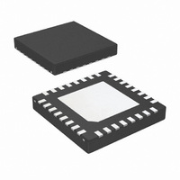
IC TRANSCEIVER M-LVDS QUAD 32LLP
Manufacturer
National Semiconductor
Type
Transceiverr
Datasheet
1.DS91M040TSQNOPB.pdf
(16 pages)
Specifications of DS91M040TSQ/NOPB
Number Of Drivers/receivers
4/4
Protocol
LVDS
Voltage - Supply
3 V ~ 3.6 V
Mounting Type
Surface Mount
Package / Case
32-LLP
Device Type
Transceiver
Supply Current Max
67mA
Signaling Rate
250Mbps
Output Level Type
LVCMOS
Supply Voltage Range
3V To 3.6V
Esd Hbm
8kV
Operating Temperature Range
-40°C To +85°C
Rohs Compliant
Yes
For Use With
DS91M040EVK - BOARD EVALUATION DS91M040
Lead Free Status / RoHS Status
Lead free / RoHS Compliant
Other names
DS91M040TSQTR
Available stocks
Company
Part Number
Manufacturer
Quantity
Price
Company:

Part Number:
DS91M040TSQ/NOPB
Manufacturer:
TI
Quantity:
1 710
Part Number:
DS91M040TSQ/NOPB
Manufacturer:
TI/德州仪器
Quantity:
20 000


M-LVDS Bus (Input and Output) Pins
I
I
I
I
I
I
C
C
C
C
SUPPLY CURRENT (V
I
I
I
I
A
B
AB
A(OFF)
B(OFF)
AB(OFF)
CCD
CCZ
CCR
CCPD
Symbol
A
B
AB
A/B
Note 4: “Absolute Maximum Ratings” indicate limits beyond which damage to the device may occur, including inoperability and degradation of device reliability
and/or performance. Functional operation of the device and/or non-degradation at the Absolute Maximum Ratings or other conditions beyond those indicated in
the Recommended Operating Conditions is not implied. The Recommended Operating Conditions indicate conditions at which the device is functional and the
device should not be operated beyond such conditions.
Note 5: The Electrical Characteristics tables list guaranteed specifications under the listed Recommended Operating Conditions except as otherwise modified
or specified by the Electrical Characteristics Conditions and/or Notes. Typical specifications are estimations only and are not guaranteed.
Note 6: Current into device pins is defined as positive. Current out of device pins is defined as negative. All voltages are referenced to ground except V
ΔV
Note 7: Typical values represent most likely parametric norms for V
product characterization and are not guaranteed.
Note 8: Output short circuit current (I
Note 9: C
OD
.
L
includes fixture capacitance and C
Transceiver input/output current
Transceiver input/output current
Transceiver input/output differential current (I
Transceiver input/output power-off current
Transceiver input/output power-off current
Transceiver input/output power-off differential
current (I
Transceiver input/output capacitance
Transceiver input/output capacitance
Transceiver input/output differential capacitance
Transceiver input/output capacitance balance
(C
Driver Supply Current
TRI-STATE Supply Current
Receiver Supply Current
Power Down Supply Current
A
/C
B
)
A(OFF)
CC
)
− I
B(OFF)
Parameter
OS
) is specified as magnitude only, minus sign indicates direction only.
)
D
includes probe capacitance.
A
DD
− I
= +3.3V and T
B
) V
V
V
V
V
V
V
V
DE = 0V
0V
V
DE = 0V
0V
V
DE = 0V
0V
V
DE = 0V
0V
V
DE = 0V
0V
V
DE = 0V
0V
V
DE = 0V
0V
V
R
DE = L, RE = H
DE = L, RE = L
MDE = L
5
A
A
A
B
B
B
A
A
A
A
B
B
B
A
DD
L
= 50Ω, DE = H, RE = H
= 3.8V, V
= 0V or 2.4V, V
= −1.4V, V
= 3.8V, V
= 0V or 2.4V, V
= −1.4V, V
= V
= 3.8V, V
= 0V or 2.4V, V
= −1.4V, V
= 3.8V, V
= 0V or 2.4V, V
= −1.4V, V
= V
≤
≤
≤
≤
≤
≤
≤
= OPEN
V
V
V
V
V
V
V
A
B
B
DD
DD
DD
DD
DD
DD
DD
= +25°C, and at the Recommended Operation Conditions at the time of
, −1.4V
, −1.4V
≤
≤
≤
≤
≤
≤
≤
Conditions
1.5V
1.5V
1.5V
1.5V
1.5V
1.5V
1.5V
B
A
B
A
B
A
B
A
= 1.2V
= 1.2V
= 1.2V,
= 1.2V,
= 1.2V
= 1.2V
≤
= 1.2V,
= 1.2V,
≤
V
V
B
A
B
A
≤
≤
= 1.2V
= 1.2V
= 1.2V,
= 1.2V,
3.8V
3.8V,
Min
−20
−32
−20
−32
−20
−32
−20
−32
−4
−4
Typ
7.8
7.8
67
22
32
3
1
3
www.national.com
Max
+20
+20
+20
+20
32
32
+4
32
32
+4
75
26
38
5
OD
Units
and
mA
mA
mA
mA
µA
µA
µA
µA
µA
µA
µA
µA
µA
µA
µA
µA
µA
µA
pF
pF
pF
Related parts for DS91M040TSQ/NOPB
Image
Part Number
Description
Manufacturer
Datasheet
Request
R

Part Number:
Description:
National Semiconductor [8-Bit D/A Converter]
Manufacturer:
National Semiconductor
Datasheet:
Part Number:
Description:
National Semiconductor [Media Coprocessor]
Manufacturer:
National Semiconductor
Datasheet:
Part Number:
Description:
Digitally Controlled Tone and Volume Circuit with Stereo Audio Power Amplifier, Microphone Preamp Stage and National 3D Sound
Manufacturer:
National Semiconductor
Datasheet:
Part Number:
Description:
Digitally Controlled Tone and Volume Circuit with Stereo Audio Power Amplifier, Microphone Preamp Stage and National 3D Sound
Manufacturer:
National Semiconductor
Datasheet:
Part Number:
Description:
AC97 Rev 2 Codec with Sample Rate Conversion and National 3D Sound
Manufacturer:
National Semiconductor
Part Number:
Description:
Manufacturer:
National Semiconductor
Datasheet:
Part Number:
Description:
Manufacturer:
National Semiconductor
Datasheet:
Part Number:
Description:
General Purpose, Low Voltage, Low Power, Rail-to-Rail Output Operational Amplifiers
Manufacturer:
National Semiconductor
Datasheet:
Part Number:
Description:
8-bit 20 MSPS flash A/D converter.
Manufacturer:
National Semiconductor
Datasheet:
Part Number:
Description:
Low Noise Quad Operational Amplifier
Manufacturer:
National Semiconductor
Datasheet:
Part Number:
Description:
Quad Differential Line Receivers
Manufacturer:
National Semiconductor
Datasheet:
Part Number:
Description:
Quad High Speed Trapezoidal? Bus Transceiver
Manufacturer:
National Semiconductor
Datasheet:
Part Number:
Description:
Dual Line Receiver
Manufacturer:
National Semiconductor
Datasheet:
Part Number:
Description:
TTL to 10k ECL Level Translator with Latch
Manufacturer:
National Semiconductor
Datasheet: