DS90CF364AMTD/NOPB National Semiconductor, DS90CF364AMTD/NOPB Datasheet - Page 3
DS90CF364AMTD/NOPB
Manufacturer Part Number
DS90CF364AMTD/NOPB
Description
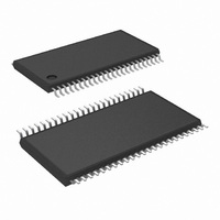
IC RCVR LVDS FPD 18BIT 48-TSSOP
Manufacturer
National Semiconductor
Type
Driverr
Datasheets
1.DS90CF364AMTDNOPB.pdf
(14 pages)
2.DS90CF364MTD.pdf
(16 pages)
3.DS90CF364MTDNOPB.pdf
(16 pages)
Specifications of DS90CF364AMTD/NOPB
Number Of Drivers/receivers
1/0
Protocol
RS644
Voltage - Supply
3 V ~ 3.6 V
Mounting Type
Surface Mount
Package / Case
48-TSSOP
Number Of Drivers
21
Number Of Receivers
3
Data Rate
1300 Mbps
Operating Supply Voltage
3.3 V
Maximum Power Dissipation
1890 mW
Maximum Operating Temperature
+ 70 C
Minimum Operating Temperature
- 10 C
Mounting Style
SMD/SMT
Supply Voltage (max)
3.6 V
Supply Voltage (min)
3 V
Supply Current
60mA
Supply Voltage Range
3V To 3.6V
Driver Case Style
TSSOP
No. Of Pins
48
Operating Temperature Range
-10°C To +70°C
Msl
MSL 2 - 1 Year
Bandwidth
170GHz
Rohs Compliant
Yes
Lead Free Status / RoHS Status
Lead free / RoHS Compliant
Other names
*DS90CF364AMTD
*DS90CF364AMTD/NOPB
DS90CF364AMTD
*DS90CF364AMTD/NOPB
DS90CF364AMTD
Available stocks
Company
Part Number
Manufacturer
Quantity
Price
Company:

Part Number:
DS90CF364AMTD/NOPB
Manufacturer:
TI
Quantity:
106


Symbol
CMOS/TTL DC SPECIFICATIONS
V
V
V
V
V
I
I
LVDS DC SPECIFICATIONS
V
V
I
I
V
V
I
TRANSMITTER SUPPLY CURRENT
ICCTW
ICCTG
IN
OS
OS
OZ
IN
Over recommended operating supply and temperature ranges unless otherwise specified.
V
V
Electrical Characteristics
IH
IL
OH
OL
CL
OD
OS
TH
TL
Absolute Maximum Ratings
If Military/Aerospace specified devices are required,
please contact the National Semiconductor Sales Office/
Distributors for availability and specifications.
Supply Voltage (V
CMOS/TTL Input Voltage
CMOS/TTL Output Voltage
LVDS Receiver Input Voltage
LVDS Driver Output Voltage
LVDS Output Short Circuit
Junction Temperature
Storage Temperature
Lead Temperature
OD
OS
Maximum Package Power Dissipation Capacity 25˚C
Duration
(Soldering, 4 sec)
MTD48 (TSSOP) Package:
High Level Input Voltage
Low Level Input Voltage
High Level Output Voltage
Low Level Output Voltage
Input Clamp Voltage
Input Current
Output Short Circuit Current
Differential Output Voltage
Change in V
complimentary output states
Offset Voltage (Note 4)
Change in V
complimentary output states
Output Short Circuit Current
Output TRI-STATE
Differential Input High Threshold
Differential Input Low Threshold
Input Current
Transmitter Supply Current, Worst
Case
Transmitter Supply Current, 16
Grayscale
CC
)
OD
Parameter
OS
between
between
®
Current
−0.3V to (V
−0.3V to (V
−0.3V to (V
−0.3V to (V
−65˚C to +150˚C
(Note 1)
−0.3V to +4V
I
I
I
V
V
R
V
PWR DWN = 0V,
V
V
V
V
R
C
Case Pattern (Figures
1, 3 ) , T
+85˚C
R
C
Grayscale Pattern
(Figures 2, 3 ) , T
−40˚C to +85˚C
Continuous
OH
OL
CL
CC
CC
CC
CC
IN
OUT
L
OUT
OUT
CM
IN
IN
L
L
L
L
= 100
= 100 ,
= 5 pF, Worst
= 100 ,
= 5 pF, 16
= 2 mA
= −18 mA
+150˚C
+260˚C
= −0.4 mA
= V
= +2.4V, V
= 0V, V
+ 0.3V)
+ 0.3V)
+ 0.3V)
+ 0.3V)
= +1.2V
= 0V
= 0V, R
= 0V or V
CC
A
, GND, 2.5V or 0.4V
= −40˚C to
CC
3
L
Conditions
CC
= 3.6V
= 100
CC
Package Derating:
ESD Rating
Recommended Operating
Conditions
Supply Voltage (V
Operating Free Air
Receiver Input Range
Supply Noise Voltage (V
A
= 3.6V
DS90C363
DS90CF364
(HBM, 1.5 k , 100 pF)
Temperature (T
=
DS90C363
DS90CF364
f = 32.5 MHz
f = 37.5 MHz
f = 65 MHz
f = 32.5 MHz
f = 37.5 MHz
f = 65 MHz
A
CC
)
)
CC
)
1.125
GND
−100
Min
250
2.0
2.7
Min
−40
3.0
0
−0.79
±
0.06
1.25
−3.5
Typ
−60
345
3.3
16 mW/˚C above +25˚C
15 mW/˚C above +25˚C
Nom
±
31
32
42
23
28
31
5.1
+25
3.3
1
1.375
−120
+100
Max
+85
Max
−1.5
100
V
±
±
±
±
3.6
2.4
450
0.8
0.3
35
35
−5
45
50
55
35
40
45
CC
10
10
10
10
www.national.com
Units
mV
1.98 W
1.89 W
>
Units
mA
mV
mV
mV
mA
mV
mV
mA
mA
mA
mA
mA
mA
˚C
µA
µA
µA
µA
V
V
V
V
V
V
V
V
7 kV
PP
Related parts for DS90CF364AMTD/NOPB
Image
Part Number
Description
Manufacturer
Datasheet
Request
R

Part Number:
Description:
National Semiconductor [8-Bit D/A Converter]
Manufacturer:
National Semiconductor
Datasheet:
Part Number:
Description:
National Semiconductor [Media Coprocessor]
Manufacturer:
National Semiconductor
Datasheet:
Part Number:
Description:
Digitally Controlled Tone and Volume Circuit with Stereo Audio Power Amplifier, Microphone Preamp Stage and National 3D Sound
Manufacturer:
National Semiconductor
Datasheet:
Part Number:
Description:
Digitally Controlled Tone and Volume Circuit with Stereo Audio Power Amplifier, Microphone Preamp Stage and National 3D Sound
Manufacturer:
National Semiconductor
Datasheet:
Part Number:
Description:
AC97 Rev 2 Codec with Sample Rate Conversion and National 3D Sound
Manufacturer:
National Semiconductor
Part Number:
Description:
Manufacturer:
National Semiconductor
Datasheet:
Part Number:
Description:
Manufacturer:
National Semiconductor
Datasheet:
Part Number:
Description:
General Purpose, Low Voltage, Low Power, Rail-to-Rail Output Operational Amplifiers
Manufacturer:
National Semiconductor
Datasheet:
Part Number:
Description:
8-bit 20 MSPS flash A/D converter.
Manufacturer:
National Semiconductor
Datasheet:
Part Number:
Description:
Low Noise Quad Operational Amplifier
Manufacturer:
National Semiconductor
Datasheet:
Part Number:
Description:
Quad Differential Line Receivers
Manufacturer:
National Semiconductor
Datasheet:
Part Number:
Description:
Quad High Speed Trapezoidal? Bus Transceiver
Manufacturer:
National Semiconductor
Datasheet:
Part Number:
Description:
Dual Line Receiver
Manufacturer:
National Semiconductor
Datasheet:
Part Number:
Description:
TTL to 10k ECL Level Translator with Latch
Manufacturer:
National Semiconductor
Datasheet: