DP83849CVS/NOPB National Semiconductor, DP83849CVS/NOPB Datasheet - Page 30
DP83849CVS/NOPB
Manufacturer Part Number
DP83849CVS/NOPB
Description
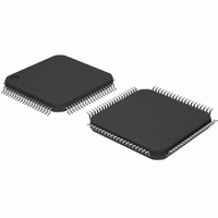
IC TXRX ETHERNET PHY DUAL 80TQFP
Manufacturer
National Semiconductor
Type
Transceiverr
Specifications of DP83849CVS/NOPB
Number Of Drivers/receivers
2/2
Protocol
Ethernet
Voltage - Supply
3 V ~ 3.6 V
Mounting Type
Surface Mount
Package / Case
80-TQFP, 80-VQFP
Data Rate
100Mbps
Supply Voltage Range
3V To 3.6V
Logic Case Style
TQFP
No. Of Pins
80
Operating Temperature Range
0°C To +70°C
Msl
MSL 3 - 168 Hours
Filter Terminals
SMD
Rohs Compliant
Yes
Data Rate Max
10Mbps
For Use With
DP83849CVS-EVK - BOARD EVALUATION DP83849CVS
Lead Free Status / RoHS Status
Lead free / RoHS Compliant
Other names
*DP83849CVS
*DP83849CVS/NOPB
DP83849CVS
*DP83849CVS/NOPB
DP83849CVS
Available stocks
Company
Part Number
Manufacturer
Quantity
Price
Company:

Part Number:
DP83849CVS/NOPB
Manufacturer:
NS
Quantity:
618
Company:
Part Number:
DP83849CVS/NOPB
Manufacturer:
Texas Instruments
Quantity:
10 000


www.national.com
3.6 802.3u MII Serial Management Interface
3.6.1 Serial Management Register Access
The serial management MII specification defines a set of
thirty-two 16-bit status and control registers that are acces-
sible through the management interface pins MDC and
MDIO. The DP83849I implements all the required MII reg-
isters as well as several optional registers. These registers
are fully described in Section 7.0. A description of the serial
management access protocol follows.
3.6.2 Serial Management Access Protocol
The serial control interface consists of two pins, Manage-
ment Data Clock (MDC) and Management Data Input/Out-
put (MDIO). MDC has a maximum clock rate of 25 MHz
and no minimum rate. The MDIO line is bi-directional and
may be shared by up to 32 devices. The MDIO frame for-
mat is shown below in Table 12.
In addition, the MDIO pin requires a pull-up resistor (1.5
k ) which, during IDLE and turnaround, will pull MDIO
high. In order to initialize the MDIO interface, the station
management entity sends a sequence of 32 contiguous
logic ones on MDIO to provide the DP83849I with a
sequence that can be used to establish synchronization.
This preamble may be generated either by driving MDIO
high for 32 consecutive MDC clock cycles, or by simply
allowing the MDIO pull-up resistor to pull the MDIO pin high
during which time 32 MDC clock cycles are provided. In
addition 32 MDC clock cycles should be used to re-sync
the device if an invalid start, opcode, or turnaround bit is
detected.
Read Operation
Write Operation
MII Management
MDIO
MDIO
MDC
Serial Protocol
(STA)
(PHY)
Z
Idle
Z
0
Start
1 1
Opcode
(Read)
0 0
(PHYAD = 0Ch)
PHY Address
1 1 0 0 0 0 0 0 0
<idle><start><op code><device addr><reg addr><turnaround><data><idle>
Figure 5. Typical MDC/MDIO Read Operation
<idle><01><10><AAAAA><RRRRR><Z0><xxxx xxxx xxxx xxxx><idle>
<idle><01><01><AAAAA><RRRRR><10><xxxx xxxx xxxx xxxx><idle>
Table 12. Typical MDIO Frame Format
Register Address
(00h = BMCR)
Z
Z
Z
30
TA
0 0 0 1 1 0 0 0 1 0 0 0 0 0 0 0 0
The DP83849I waits until it has received this preamble
sequence before responding to any other transaction.
Once the DP83849I serial management port has been ini-
tialized no further preamble sequencing is required until
after a power-on/reset, invalid Start, invalid Opcode, or
invalid turnaround bit has occurred.
The Start code is indicated by a <01> pattern. This assures
the MDIO line transitions from the default idle line state.
Turnaround is defined as an idle bit time inserted between
the Register Address field and the Data field. To avoid con-
tention during a read transaction, no device shall actively
drive the MDIO signal during the first bit of Turnaround.
The addressed DP83849I drives the MDIO with a zero for
the second bit of turnaround and follows this with the
required data. Figure 5 shows the timing relationship
between MDC and the MDIO as driven/received by the Sta-
tion (STA) and the DP83849I (PHY) for a typical register
read access.
For write transactions, the station management entity
writes data to the addressed DP83849I thus eliminating the
requirement for MDIO Turnaround. The Turnaround time is
filled by the management entity by inserting <10>. Figure 6
shows the timing relationship for a typical MII register write
access.
Register Data
Z
Idle
Z
Related parts for DP83849CVS/NOPB
Image
Part Number
Description
Manufacturer
Datasheet
Request
R

Part Number:
Description:
National Semiconductor [8-Bit D/A Converter]
Manufacturer:
National Semiconductor
Datasheet:
Part Number:
Description:
National Semiconductor [Media Coprocessor]
Manufacturer:
National Semiconductor
Datasheet:
Part Number:
Description:
Digitally Controlled Tone and Volume Circuit with Stereo Audio Power Amplifier, Microphone Preamp Stage and National 3D Sound
Manufacturer:
National Semiconductor
Datasheet:
Part Number:
Description:
Digitally Controlled Tone and Volume Circuit with Stereo Audio Power Amplifier, Microphone Preamp Stage and National 3D Sound
Manufacturer:
National Semiconductor
Datasheet:
Part Number:
Description:
AC97 Rev 2 Codec with Sample Rate Conversion and National 3D Sound
Manufacturer:
National Semiconductor
Part Number:
Description:
Manufacturer:
National Semiconductor
Datasheet:
Part Number:
Description:
Manufacturer:
National Semiconductor
Datasheet:
Part Number:
Description:
General Purpose, Low Voltage, Low Power, Rail-to-Rail Output Operational Amplifiers
Manufacturer:
National Semiconductor
Datasheet:
Part Number:
Description:
8-bit 20 MSPS flash A/D converter.
Manufacturer:
National Semiconductor
Datasheet:
Part Number:
Description:
Low Noise Quad Operational Amplifier
Manufacturer:
National Semiconductor
Datasheet:
Part Number:
Description:
Quad Differential Line Receivers
Manufacturer:
National Semiconductor
Datasheet:
Part Number:
Description:
Quad High Speed Trapezoidal? Bus Transceiver
Manufacturer:
National Semiconductor
Datasheet:
Part Number:
Description:
Dual Line Receiver
Manufacturer:
National Semiconductor
Datasheet:
Part Number:
Description:
TTL to 10k ECL Level Translator with Latch
Manufacturer:
National Semiconductor
Datasheet: