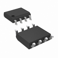
CLC006BM/NOPB National Semiconductor, CLC006BM/NOPB Datasheet - Page 4

CLC006BM/NOPB
Manufacturer Part Number
CLC006BM/NOPB
Description
IC CABLE DVR DGTL SER ADJ 8-SOIC
Manufacturer
National Semiconductor
Series
CLCr
Type
Driverr
Datasheet
1.CLC006BMNOPB.pdf
(12 pages)
Specifications of CLC006BM/NOPB
Number Of Drivers/receivers
1/0
Voltage - Supply
4.5 V ~ 5.5 V
Mounting Type
Surface Mount
Package / Case
8-SOIC (3.9mm Width)
Leaded Process Compatible
Yes
Rohs Compliant
Yes
Peak Reflow Compatible (260 C)
Yes
For Use With
SD901EVK - BOARD EVAL CLC014, 016, 011, 006SD006EVK - BOARD EVALUATION CLC006
Lead Free Status / RoHS Status
Lead free / RoHS Compliant
Protocol
-
Other names
CLC006BM
www.national.com
Operation
INPUT INTERFACING
The CLC006 has high impedance, emitter-follower buffered,
differential inputs. Single-ended signals may also be input.
Transmission lines supplying input signals must be properly
terminated close to the CLC006. Either A.C. or D.C. coupling
as in Figure 2 or Figure 3 may be used.Figures 2, 4 and Figure
5 show how Thevenin-equivalent resistor networks are used
ECL, 50Ω, 5V, V
ECL, 50Ω, 5.2V, V
ECL, 75Ω, 5V, V
ECL, 75Ω, 5.2V, V
800 mV
800 mV
800 mV
P-P
P-P
P-P
, 50Ω, 5V, V
, 75Ω, 5V, V
, 2.2KΩ, 5Ω, V
T
T
=2V
=2V
T
T
=2V
=2V
Load Type
T
T
=1.6V
=1.6V
T
=1.6V
FIGURE 2. AC Coupled Input
FIGURE 1. Input Stage
Resistor to V
4
to provide input termination and biasing. The input D.C. com-
mon-mode voltage range is 0.8V to 2.5V below the positive
power supply (V
within the specified common-mode range. For an 800 mV
input signal, typical input bias levels range from 1.2V to 2.1V
below the positive supply.
3240Ω
82.5Ω
80.6Ω
75.0Ω
124Ω
121Ω
110Ω
10008404
CC
(R1)
CC
). Input signals plus bias should be kept
10008405
Resistor to V
6810Ω
124Ω
133Ω
187Ω
196Ω
154Ω
232Ω
EE
(R2)
P-P


