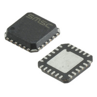
LAN8700IC-AEZG SMSC, LAN8700IC-AEZG Datasheet - Page 13

LAN8700IC-AEZG
Manufacturer Part Number
LAN8700IC-AEZG
Description
TXRX ETHERNET 10/100 IND 36-QFN
Manufacturer
SMSC
Type
Transceiverr
Datasheet
1.LAN8700C-AEZG.pdf
(80 pages)
Specifications of LAN8700IC-AEZG
Protocol
MII, RMII
Voltage - Supply
3 V ~ 3.6 V
Mounting Type
Surface Mount
Package / Case
36-QFN
Supply Voltage Range
3V To 3.6V
Digital Ic Case Style
QFN
No. Of Pins
36
Operating Temperature Range
-40°C To +85°C
Control Interface
MII, RMII
Data Rate Max
100Mbps
Rohs Compliant
Yes
Lead Free Status / RoHS Status
Lead free / RoHS Compliant
Number Of Drivers/receivers
-
Other names
638-1047-6
Available stocks
Company
Part Number
Manufacturer
Quantity
Price
Company:
Part Number:
LAN8700IC-AEZG
Manufacturer:
SANKEN
Quantity:
300
Company:
Part Number:
LAN8700IC-AEZG
Manufacturer:
Standard
Quantity:
34 317
Part Number:
LAN8700IC-AEZG
Manufacturer:
SMSC
Quantity:
20 000
Part Number:
LAN8700IC-AEZG-C3
Manufacturer:
SMSC
Quantity:
20 000
Part Number:
LAN8700IC-AEZG-TR
Manufacturer:
MICROCHIP/微芯
Quantity:
20 000
±15kV ESD Protected MII/RMII 10/100 Ethernet Transceiver with HP Auto-MDIX Support and flexPWR
Datasheet
SMSC LAN8700/LAN8700i
SIGNAL NAME
nINTSEL
TX_CLK
MODE0
MODE1
MODE2
RXD0/
RXD1/
RXD2/
RXD3/
TYPE
IOPU
IOPU
IOPU
IOPU
Table 3.1 MII Signals (continued)
O
DATASHEET
Transmit Clock: 25MHz in 100Base-TX mode. 2.5MHz in
10Base-T mode.
Note:
Note:
Receive Data 0: Bit 0 of the 4 data bits that are sent by the PHY
in the receive path.
PHY Operating Mode Bit 0: set the default MODE of the PHY.
Note:
Receive Data 1: Bit 1 of the 4 data bits that are sent by the PHY
in the receive path.
PHY Operating Mode Bit 1: set the default MODE of the PHY.
Note:
Receive Data 2: Bit 2 of the 4 data bits that are sent by the PHY
in the receive path.
PHY Operating Mode Bit 2: set the default MODE of the PHY.
Notes:
Receive Data 3: Bit 3 of the 4 data bits that are sent by the PHY
in the receive path.
nINTSEL: On power-up or external reset, the mode of the
nINT/TXER/TXD4 pin is selected.
Notes:
RXD2 is not used in RMII Mode.
See
the MODE options.
When RXD3/nINTSEL is floated or pulled to VDDIO, nINT is
selected for operation on pin nINT/TXER/TXD4 (default).
When RXD3/nINTSEL is pulled low to VSS through a resistor,
(see
page
nINT/TXER/TXD4.
RXD3 is not used in RMII Mode
If the nINT/TXER/TXD4 pin is configured for nINT mode, then
a pull-up resistor is needed to VDDIO on the nINT/TXER/TXD4
pin. see
page
See
for additional information on configuration/strapping options.
®
Section 5.4.9.2, "Mode Bus – MODE[2:0]," on page
Section 4.10, "nINT/TX_ER/TXD4 Strapping," on page 31
13
Table 4.3, “Boot Strapping Configuration Resistors,” on
Technology in a Small Footprint
32), TXER/TXD4 is selected for operation on pin
32.
This signal is not used in RMII Mode.
For proper TXCLK operation, RX_ER and RX_DV must
NOT be driven high externally on a hardware reset or
on a LAN8700 power up.
See
page
See
page
Table 4.3, “Boot Strapping Configuration Resistors,” on
Section 5.4.9.2, "Mode Bus – MODE[2:0]," on
Section 5.4.9.2, "Mode Bus – MODE[2:0]," on
54, for the MODE options
54, for the MODE options.
DESCRIPTION
Revision 2.2 (12-04-09)
54, for


