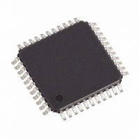
DS2148T+ Maxim Integrated Products, DS2148T+ Datasheet - Page 34

DS2148T+
Manufacturer Part Number
DS2148T+
Description
IC LIU E1/T1/J1 5V 44-TQFP
Manufacturer
Maxim Integrated Products
Type
Line Interface Units (LIUs)r
Specifications of DS2148T+
Number Of Drivers/receivers
1/1
Protocol
T1/E1/J1
Voltage - Supply
4.75 V ~ 5.25 V
Mounting Type
Surface Mount
Package / Case
44-TQFP, 44-VQFP
Lead Free Status / RoHS Status
Lead free / RoHS Compliant
5 STATUS REGISTERS
There are three registers that contain information on the current real-time status of the device, status
register (SR), and receive information registers 1 and 2 (RIR1/RIR2). When a particular event has
occurred (or is occurring), the appropriate bit in one of these three registers will be set to a one. Some of
the bits in SR, RIR1, and RIR2 are latched bits and some are real-time bits. The register descriptions
below list which status bits are latched and which are real-time bits. For latched status bits, when an event
or an alarm occurs the bit is set to a one and will remain set until the user reads that bit. The bit will be
cleared when it is read and it will not be set again until the event has occurred again. Two of the latched
status bits (RUA1 & RCL) will remain set after reading if the alarm is still present.
The user will always precede a read of any of the three status registers with a write. The byte written to
the register will inform the DS2148 which bits the user wishes to read and have cleared. The user will
write a byte to one of these registers with a one in the bit positions to be read and a zero in the other bit
positions. When a one is written to a bit location, that location will be updated with the latest information.
When a zero is written to a bit position, that bit position will not be updated and the previous value will
be held. A write to the status and information registers will be immediately followed by a read of the
same register. The read result should be logically ANDed with the mask byte that was just written and
this value should be written back into the same register to ensure that bit does indeed clear. This second
write step is necessary because the alarms and events in the status registers occur asynchronously with
respect to their access via the parallel port. This write-read-write scheme allows an external
microcontroller or microprocessor to individually poll certain bits without disturbing the other bits in the
register. This operation is key in controlling the DS2148 with higher-order software languages.
The bits in the SR register have the unique ability to initiate a hardware interrupt via the INT output pin.
Each of the alarms and events in the SR can be either masked or unmasked from the interrupt pin via the
interrupt mask register (IMR). The interrupts caused by the RCL, RUA1, and LOTC bits in SR act
differently than the interrupts caused by the other status bits in SR. The RCL, RUA1 and LOTC bits will
force the INT pin low whenever they change state (i.e., go active or inactive). The INT pin will be
allowed to return high (if no other interrupts are present) when the user reads the alarm bit that caused the
interrupt to occur even if the alarm is still present. The other status bits in SR can force the INT pin low
when they are set. The INT pin will be allowed to return high (if no other interrupts are present) when the
user reads the event bit that caused the interrupt to occur.
SYMBOL
ECRS2
ECRS1
ECRS0
RJAB
POSITION
CCR6.3
CCR6.2
CCR6.1
CCR6.0
DESCRIPTION
RCLK Jitter Attenuator Bypass. This control bit allows the recovered
received clock and data to bypass the jitter attenuation while still
allowing the BPCLK output to use the jitter attenuator. See
and Section
0 = disabled
1 = enabled
Error Count Register Select 2. See Section
Error Count Register Select 1. See Section
Error Count Register Select 0. See Section
7.1
for details.
34 of 73
6.4
6.4
6.4
for details.
for details.
for details.
Figure 1-1


