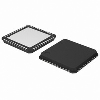
AMIS-49200-XTD ON Semiconductor, AMIS-49200-XTD Datasheet - Page 9

AMIS-49200-XTD
Manufacturer Part Number
AMIS-49200-XTD
Description
TXRX FIELDBUS MAU 44-LQFP
Manufacturer
ON Semiconductor
Type
Transceiverr
Specifications of AMIS-49200-XTD
Number Of Drivers/receivers
1/1
Protocol
MDS-MAU
Voltage - Supply
4.75 V ~ 6.2 V
Mounting Type
Surface Mount
Package / Case
44-LQFP
Logic Type
Fieldbus Media Access Unit
Logic Family
AMIS-49200
Input Level
CMOS
Supply Voltage (max)
6.2 V
Supply Voltage (min)
3 V
Maximum Operating Temperature
+ 85 C
Function
A transceiver chip for low speed FOUNDATION Fieldbus and Profibus PA devices
Minimum Operating Temperature
- 40 C
Mounting Style
SMD/SMT
Lead Free Status / RoHS Status
Lead free / RoHS Compliant
Other names
766-1019
Available stocks
Company
Part Number
Manufacturer
Quantity
Price
Company:
Part Number:
AMIS-49200-XTD
Manufacturer:
ON Semiconductor
Quantity:
31
Company:
Part Number:
AMIS-49200-XTD
Manufacturer:
ON Semiconductor
Quantity:
10 000
AMIS-492x0
3.3 Transmitter Blocks
Table 7: MDS-MAU Interface
Note: The associated MDS chip must handle the jabber detect function.
Table 8: Tri-level Modulator
Notes:
Table 9: Current Control Amplifier
Parameter
MDS-MAU Interface
POL input pin
TxE input pin
TxS input pin
Parameter
Tri-level Modulator and Slew Control
Output voltage
Load current
Output for silence
Output for high level
Output for low level
Asymmetry of V
Rise and fall times
Parameter
Current Control Amplifier
Input common mode voltage
range
Output voltage swing
Load current
Input offset voltage
Slew rate
Gain bandwidth product
Phase margin
1.
2.
Nominal values are: V
By adding an external capacitor between the CRT pin and ground, slew rate at VDRV output can be controlled. The controlling equation is tf or tr = 2us +
(0.123us/pF * C
should have a guard pattern around them to avoid unnecessary interference.
H
and V
(1)
(2)
(1)
(1)
RT
L
). C
S
RT
= 2.5V, V
is nominally 22pF, yielding tf = tr =4.7us. The constant comes from an internal capacitor. The hot side of the capacitor and the CRT pin
Symbol
Symbol
GBW
∆V
H
tf, tr
V
V
PM
SR
V
V
V
V
V
= 2.9V and V
I
I
Symbol
O
CM
OS
o
O
H
O
S
L
HL
POL
TxE
TxS
V
L
V
V
= 2.1V.
MID
-2300
Min.
S
S
-0.02
Min.
+0.380
-3
V
-0.420
0
1
-35
See Schmitt Trigger input specs
+0.485
MID
Min.
Rev. 6 | Page 9 of 22 | www.onsemi.com
Typ.
V
Typ.
0.54
1.15
V
66
V
MID
S
S
Typ.
+0.400
-0.400
4.7
+0.500
Max.
V
V
CC
Max.
V
CC
100
V
V
+3
MID
– 0.5
S
S
– 1
Max.
+120
3.02
+0.420
0.02
-0.380
+0.515
Units
V
V
V
Units
MHz
V/μs
Deg
mV
μA
V
V
Units
μsec
μA
Conditions
V
V
V
V
V
Conditions
(Output is at CCOUT)
C
R
L
L
Conditions
(Output is at VDRV)
|∆V| 10mV
TXE disabled
TXE active
TXE active
Note 2
(C
= 10pf
= 200k
RT
= 22pF)


