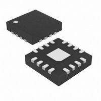
MAX3982UTE+ Maxim Integrated Products, MAX3982UTE+ Datasheet - Page 10

MAX3982UTE+
Manufacturer Part Number
MAX3982UTE+
Description
IC DRIVER SFP CABLE 16-TQFN
Manufacturer
Maxim Integrated Products
Type
Driverr
Datasheet
1.MAX3982UTE.pdf
(15 pages)
Specifications of MAX3982UTE+
Number Of Drivers/receivers
1/0
Voltage - Supply
3 V ~ 3.6 V
Mounting Type
Surface Mount
Package / Case
16-TQFN Exposed Pad
Maximum Operating Temperature
+ 85 C
Mounting Style
SMD/SMT
Minimum Operating Temperature
0 C
Lead Free Status / RoHS Status
Lead free / RoHS Compliant
Protocol
-
Lead Free Status / Rohs Status
Details
SFP Copper-Cable Preemphasis Driver
10
4, 8, 9
12, 13
PIN
10
11
14
15
16
EP
______________________________________________________________________________________
1
2
3
5
6
7
*THE EXPOSED PAD OF THE QFN PACKAGE MUST BE SOLDERED TO GROUND
FOR PROPER THERMAL OPERATION OF THE MAX3982.
TOP VIEW
V
GND
TX_DISABLE
CC1
IN+
IN-
EXPOSED
OUTLEV
LOSLEV
NAME
OUT+
V
OUT-
V
GND
PAD
LOS
PE1
PE0
IN+
1
2
3
4
IN-
CC1
CC2
16
5
MAX3982UTE
EXPOSED PAD*
THIN QFN
15
6
Power-Supply Connection for Input. Connect to +3.3V.
Positive Data Input, CML. This input is internally terminated with 50 to V
Negative Data Input, CML. This input is internally terminated with 50 to V
Circuit Ground
Output-Swing Control Input, LVTTL with 40k Internal Pullup. Set to TTL high or open for maximum
output swing, or set to TTL low for reduced swing.
Output Preemphasis Control Input, LVTTL with 10k Internal Pullup. This pin is the most significant bit
of the 2-bit preemphasis control. Set high or open to assert this bit.
Output Preemphasis Control Input, LVTTL with 10k Internal Pullup. This pin is the least significant bit
of the 2-bit preemphasis control. Set high or open to assert this bit.
Negative Data Output, CML. This output is terminated with 50 to V
Positive Data Output, CML. This output is terminated with 50 to V
Power-Supply Connection for Output. Connect to +3.3V.
Transmitter Disable Input, LVTTL with 10k Internal Pullup. When high or open, differential output is
40mV
Loss-of-Signal Detect, TTL Output. This output is open-collector TTL, and therefore requires an external
4.7k to 10k pullup resistor (5.5V maximum). This output sinks current when the input signal level is
valid.
LOS Sensitivity Control Input, LVTTL with 40k Internal Pullup. Set to TTL high or open for less
sensitivity (higher assert threshold). Set to TTL low for more sensitivity (lower assert threshold).
Exposed Pad. For optimal thermal conductivity, this pad must be soldered to the circuit board ground.
Pin Configuration
14
7
P-P
13
8
. Set low for normal operation.
12
11
10
9
V
OUT+
OUT-
GND
CC2
FUNCTION
CC2
CC2
.
.
CC1
CC1
Pin Description
.
.


