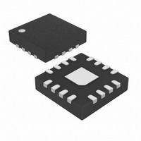
MAX3982UTE+ Maxim Integrated Products, MAX3982UTE+ Datasheet - Page 12

MAX3982UTE+
Manufacturer Part Number
MAX3982UTE+
Description
IC DRIVER SFP CABLE 16-TQFN
Manufacturer
Maxim Integrated Products
Type
Driverr
Datasheet
1.MAX3982UTE.pdf
(15 pages)
Specifications of MAX3982UTE+
Number Of Drivers/receivers
1/0
Voltage - Supply
3 V ~ 3.6 V
Mounting Type
Surface Mount
Package / Case
16-TQFN Exposed Pad
Maximum Operating Temperature
+ 85 C
Mounting Style
SMD/SMT
Minimum Operating Temperature
0 C
Lead Free Status / RoHS Status
Lead free / RoHS Compliant
Protocol
-
Lead Free Status / Rohs Status
Details
SFP Copper-Cable Preemphasis Driver
The MAX3982 can automatically detect an incoming
signal and enable the data outputs. Autodetect can be
accomplished by connecting the LOS pin to TX_DIS-
ABLE. TX_DISABLE has a 10k
If a loss-of-signal is detected, the TX_DISABLE pin is
forced high and disables the outputs. Leaving the
inputs to the MAX3982 open (i.e., floating) is not recom-
mended as noise amplification may occur and create
undesirable output signals. Autodetect is recommend-
ed to eliminate noise amplification or possible oscilla-
tion. For periods much greater than 100ns without data
transitions, autodetect disables the output.
Table 1. Preemphasis Translation
Figure 5. IN+/IN- Equivalent Input Structure
12
V
V
HIGH PP
LOW PP
______________________________________________________________________________________
Ratio
1.26
1.58
2.51
5.01
_
IN+
_
IN-
Applications Information
V
V
HIGH PP
HIGH PP
V
_
_
CC1
50
GND
0.11
0.23
0.43
0.67
V
V
LOW PP
LOW PP
50
internal pullup resistor.
_
_
Autodetect
1
10Gbase–CX4
V
V
0.21
0.37
0.6
0.8
HIGH PP
LOW PP
_
_
Circuit board layout and design can significantly affect
the performance of the MAX3982. Use good high-fre-
quency design techniques, including minimizing ground
inductance and using controlled-impedance transmis-
sion lines on the data signals. Power-supply decoupling
should also be placed as close to the V
ble. This should be sufficient supply filtering. Always con-
nect all V
the input from the output signals to reduce feedthrough.
The exposed-pad, 16-pin QFN package incorporates
features that provide a very low thermal resistance path
for heat removal from the IC. The exposed pad on the
MAX3982 must be soldered to the circuit board for
proper thermal performance. For more information on
exposed-pad packages, refer to Maxim Application
Note HFAN-08.1: Thermal Considerations of QFN and
Other Exposed-Paddle Packages.
Figure 6. OUT+/OUT- Equivalent Output Structure
20 log
V
V
IN dB
HIGH PP
CC
LOW PP
14
2
4
8
pins to a power plane. Take care to isolate
_
_
50
Interface Schematics
V
CC2
Layout Considerations
Exposed Pad Package
50
GND
V
LOW_PP
CC
pins as possi-
V
HIGH_PP
OUT+
OUT-


