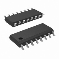
DS90C031BTMX/NOPB National Semiconductor, DS90C031BTMX/NOPB Datasheet

DS90C031BTMX/NOPB
Specifications of DS90C031BTMX/NOPB
*DS90C031BTMX/NOPB
DS90C031BTMX
Available stocks
Related parts for DS90C031BTMX/NOPB
DS90C031BTMX/NOPB Summary of contents
Page 1
... Connection Diagram Dual-In-Line Order Number DS90C031BTM See NS Package Number M16A Driver Truth Table EN L All other combinations of ENABLE inputs © 2001 National Semiconductor Corporation Features > 155.5 Mbps (77.7 MHz) switching rates n n High impedance LVDS outputs with power-off ± 350 mV differential signaling n n Ultra low power dissipation n 400 ps maximum differential skew (5V, 25˚ ...
Page 2
... Absolute Maximum Ratings If Military/Aerospace specified devices are required, please contact the National Semiconductor Sales Office/ Distributors for availability and specifications. Supply Voltage ( Input Voltage ( Enable Input Voltage (EN, EN*) Output Voltage ( OUT+ OUT− Short Circuit Duration ( OUT+ OUT− Maximum Package Power Dissipation ...
Page 3
Switching Characteristics V = +5.0V +25˚C (Notes Symbol Parameter t Rise Time TLH t Fall Time THL t Disable Time High to Z PHZ t Disable Time Low to Z PLZ t Enable ...
Page 4
Parameter Measurement Information FIGURE 2. Driver Propagation Delay and Transition Time Test Circuit FIGURE 3. Driver Propagation Delay and Transition Time Waveforms www.national.com (Continued) FIGURE 4. Driver TRI-STATE Delay Test Circuit 4 10098904 10098905 10098906 ...
Page 5
Parameter Measurement Information Typical Application Applications Information LVDS drivers and receivers are intended to be primarily used in an uncomplicated point-to-point configuration as is shown in Figure 6 . This configuration provides a clean signaling environment for the quick edge ...
Page 6
Applications Information to some ECL and PECL devices, but without the heavy static I requirements of the ECL/PECL designs. LVDS requires CC > 80% less current than similar PECL devices. AC specifi- cations for the driver are a tenfold improvement ...
Page 7
Typical Performance Characteristics Power Supply Current vs Power Supply Voltage Power Supply Current vs Power Supply Voltage Output TRI-STATE Current vs Power Supply Voltage Power Supply Current 10098910 Power Supply Current 10098912 Output Short Circuit Current vs Power Supply Voltage ...
Page 8
Typical Performance Characteristics Differential Output Voltage vs Power Supply Voltage Output Voltage High vs Power Supply Voltage Output Voltage Low vs Power Supply Voltage www.national.com (Continued) Differential Output Voltage vs Ambient Temperature 10098916 Output Voltage High vs Ambient Temperature 10098918 ...
Page 9
Typical Performance Characteristics Offset Voltage vs Power Supply Voltage Power Supply Current vs Frequency Differential Output Voltage vs Load Resistor (Continued) 10098922 10098924 Differential Propagation Delay vs Power Supply Voltage 10098926 9 Offset Voltage vs Ambient Temperature 10098923 Power Supply ...
Page 10
Typical Performance Characteristics Differential Propagation Delay vs Ambient Temperature Differential Skew vs Ambient Temperature Differential Transition Time vs Ambient Temperature www.national.com (Continued) Power Supply Voltage 10098928 Differential Transition Time vs Power Supply Voltage 10098930 10098932 10 Differential Skew vs 10098929 ...
Page 11
... NATIONAL’S PRODUCTS ARE NOT AUTHORIZED FOR USE AS CRITICAL COMPONENTS IN LIFE SUPPORT DEVICES OR SYSTEMS WITHOUT THE EXPRESS WRITTEN APPROVAL OF THE PRESIDENT AND GENERAL COUNSEL OF NATIONAL SEMICONDUCTOR CORPORATION. As used herein: 1. Life support devices or systems are devices or systems which, (a) are intended for surgical implant ...


