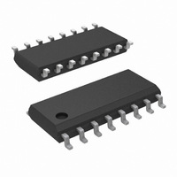
DS90C031BTMX/NOPB National Semiconductor, DS90C031BTMX/NOPB Datasheet - Page 3

DS90C031BTMX/NOPB
Manufacturer Part Number
DS90C031BTMX/NOPB
Description
IC LINE DRIVER QUAD DIFF 16-SOIC
Manufacturer
National Semiconductor
Type
Driverr
Datasheet
1.DS90C031BTMNOPB.pdf
(11 pages)
Specifications of DS90C031BTMX/NOPB
Number Of Drivers/receivers
4/0
Protocol
LVDS
Voltage - Supply
4.5 V ~ 5.5 V
Mounting Type
Surface Mount
Package / Case
16-SOIC (3.9mm Width)
Lead Free Status / RoHS Status
Lead free / RoHS Compliant
Other names
*DS90C031BTMX
*DS90C031BTMX/NOPB
DS90C031BTMX
*DS90C031BTMX/NOPB
DS90C031BTMX
Available stocks
Company
Part Number
Manufacturer
Quantity
Price
t
t
t
t
t
t
t
t
t
t
t
t
t
t
t
t
t
TLH
THL
PHZ
PLZ
PZH
PZL
PHLD
PLHD
SKD
SK1
SK2
TLH
THL
PHZ
PLZ
PZH
PZL
Symbol
Symbol
Switching Characteristics
V
Switching Characteristics
V
Note 1: “Absolute Maximum Ratings” are those values beyond which the safety of the device cannot be guaranteed. They are not meant to imply that the devices
should be operated at these limits. The table of “Electrical Characteristics” specifies conditions of device operation.
Note 2: Current into device pins is defined as positive. Current out of device pins is defined as negative. All voltages are referenced to ground except: V
Note 3: All typicals are given for: V
Note 4: Channel-to-Channel Skew is defined as the difference between the propagation delay of the channel and the other channels in the same chip with an event
on the inputs.
Note 5: Chip to Chip Skew is defined as the difference between the minimum and maximum specified differential propagation delays.
Note 6: Generator waveform for all tests unless otherwise specified: f = 1 MHz, Z
Note 7: ESD Ratings:
Note 8: Output short circuit current (I
Note 9: C
Parameter Measurement Information
V
CC
CC
OD1
HBM (1.5 k , 100 pF)
EIAJ (0 , 200 pF)
= +5.0V, T
= +5.0V
.
L
includes probe and jig capacitance.
Rise Time
Fall Time
Disable Time High to Z
Disable Time Low to Z
Enable Time Z to High
Enable Time Z to Low
Differential Propagation Delay High to Low
Differential Propagation Delay Low to High
Differential Skew |t
Channel-to-Channel Skew (Note 4)
Chip to Chip Skew (Note 5)
Rise Time
Fall Time
Disable Time High to Z
Disable Time Low to Z
Enable Time Z to High
Enable Time Z to Low
±
A
10%, T
= +25˚C (Notes 3, 6, 9)
250V
A
2kV
= −40˚C to +85˚C (Notes 3, 6, 9)
CC
Parameter
Parameter
PHLD
OS
= +5.0V, T
) is specified as magnitude only, minus sign indicates direction only.
– t
PLHD
A
= +25˚C.
FIGURE 1. Driver V
|
(Continued)
R
( Figure 4 and Figure 5 )
R
( Figure 2 and Figure 3 )
R
( Figure 4 and Figure 5 )
OD
L
L
L
3
= 100 , C
= 100 , C
= 100 , C
and V
O
= 50 , t
Conditions
Conditions
OS
r
L
L
L
Test Circuit
= 5 pF
= 5 pF
= 5 pF
6 ns, and t
f
6 ns.
Min
Min
0.5
0.5
0
0
10098903
0.35
0.35
0.35
0.35
Typ
Typ
2.5
2.5
2.5
2.5
2.0
2.1
0.3
2.5
2.5
2.5
2.5
80
Max
Max
900
1.5
1.5
3.5
3.5
1.0
3.0
2.0
2.0
10
10
10
10
15
15
15
15
www.national.com
OD1
Units
Units
ns
ns
ns
ns
ns
ns
ns
ns
ps
ns
ns
ns
ns
ns
ns
ns
ns
and


