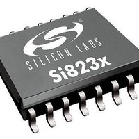
Si8230-A-IS Silicon Laboratories Inc, Si8230-A-IS Datasheet - Page 20

Si8230-A-IS
Manufacturer Part Number
Si8230-A-IS
Description
MOSFET & Power Driver ICs 0.5A HS/LS ISOdriver Dual Input
Manufacturer
Silicon Laboratories Inc
Type
High and Low Sider
Datasheet
1.SI8234BD-C-IS.pdf
(52 pages)
Specifications of Si8230-A-IS
Rise Time
12 ns
Fall Time
12 ns
Propagation Delay Time
50 ns
Supply Voltage (max)
24 V
Supply Voltage (min)
10 V
Supply Current
11 mA
Maximum Operating Temperature
+ 125 C
Mounting Style
SMD/SMT
Package / Case
SOIC-16
Bridge Type
Half Bridge
Minimum Operating Temperature
- 40 C
Number Of Drivers
2
Number Of Outputs
2
Output Current
0.5 A
Lead Free Status / Rohs Status
Lead free / RoHS Compliant
Si823x
3.3. Family Overview and Logic Operation During Startup
The Si823x family of isolated drivers consists of high-side, low-side, and dual driver configurations.
3.3.1. Products
Table 9 shows the configuration and functional overview for each product in this family.
3.3.2. Device Behavior
Table 10 contains truth tables for the Si8230/3, Si8231/4, and Si8232/5/6 families.
20
*Note: This truth table assumes VDDA and VDDB are powered. If VDDA and VDDB are below UVLO, see
Part Number
VIA
PWM Input
H
H
Si8235/6
L
L
X
X
Si8230
Si8231
Si8232
Si8233
Si8234
Inputs
"3.7.2.Undervoltage Lockout" on page 24 for more information.
H
X
X
L
VIB
H
H
X
X
L
L
High-Side/Low-Side
High-Side/Low-Side
High-Side/Low-Side
High-Side/Low-Side
VDDI State Disable
Unpowered
VDDI State Disable
Unpowered
Powered
Powered
Powered
Powered
Powered
Powered
Powered
Powered
Configuration
Dual Driver
Dual Driver
Si8231/4 (PWM Input High-Side/Low-Side) Truth Table
Si8230/3 (High-Side/Low-Side) Truth Table
Table 10. Si823x Family Truth Table*
X
H
X
H
L
L
L
L
L
L
Table 9. Si823x Family Overview
VOA
VOA
Protection
H
H
L
L
L
L
L
L
L
L
Overlap
Output
Output
—
—
VOB
VOB
Rev. 1.1
H
H
L
L
L
L
L
L
L
L
Output transition occurs after internal dead time
expires.
Output transition occurs after internal dead time
expires.
Output transition occurs after internal dead time
expires.
Invalid state. Output transition occurs after internal
dead time expires.
Output returns to input state within 7 µs of VDDI
power restoration.
Device is disabled.
Output transition occurs after internal dead time
expires.
Output transition occurs after internal dead time
expires.
Output returns to input state within 7 µs of VDDI
power restoration.
Device is disabled.
Programmable
Dead Time
—
—
Notes
Notes
VIA, VIB
VIA, VIB
VIA, VIB
VIA, VIB
Inputs
PWM
PWM
Peak Output
Current (A)
0.5
0.5
0.5
4.0
4.0
4.0


