DS92CK16TMTCX/NOPB National Semiconductor, DS92CK16TMTCX/NOPB Datasheet
DS92CK16TMTCX/NOPB
Specifications of DS92CK16TMTCX/NOPB


Related parts for DS92CK16TMTCX/NOPB

DS92CK16TMTCX/NOPB Summary of contents
Page 1
... VID≤ −0.07V L = Low Logic State H = High Logic State X = Irrelevant Z = TRI-STATE TRI-STATE ® registered trademark of National Semiconductor Corporation. © 2006 National Semiconductor Corporation Features n Master/Slave clock selection in a backplane application n 125 MHz operation (typical) n 100 ps duty cycle distortion (typical channel to channel skew (typical ...
Page 2
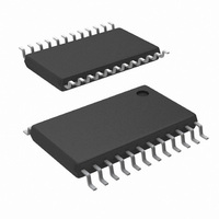
Connection Diagram TSSOP Package Pin Descriptions Pin Name Pin # CLKI/O+ 6 CLKI/O− CLK 13, 15, 17, 19, 21, 23 OUT CrdCLK 16, 20 GND 1, 12, 14, 18, 22 ...
Page 3
... Absolute Maximum Ratings If Military/Aerospace specified devices are required, please contact the National Semiconductor Sales Office/ Distributors for availability and specifications. Supply Voltage ( Enable Input Voltage (DE, OE, CrdCLK ) IN Voltage (CLK ) OUT ± Voltage (CLKI/O ) Driver Short Circuit Current Receiver Short Circuit Current Maximum Package Power Dissipation at +25˚ ...
Page 4
DC Electrical Characteristics Over Supply Voltage and Operating Temperature ranges, unless otherwise specified (Notes 3, 4). Symbol Parameter I No Load Supply Current 0V, CC Outputs Enabled, No VID CrdCLK Applied CLKI/O ( CLK I No ...
Page 5
Switching Characteristics Over Supply Voltage and Operating Temperature ranges, unless otherwise specified (Notes 7, 8). Symbol Parameter DIFFERENTIAL RECEIVER CHARACTERISTICS t Differential Propagation Delay High to Low. CLKI/O to PHLDR CLK OUT t Differential Propagation Delay Low to High. CLKI/O ...
Page 6
Switching Characteristics Note 10 the difference in receiver propagation delay (|t SK1R V . The propagation delay specification is a device to device worst case over process, voltage and temperature. CC Note 11 the difference in ...
Page 7
Parameter Measurement Information FIGURE 4. Output Enable (OE) Delay Waveforms FIGURE 6. Driver Propagation Delay Test Circuit (Continued) FIGURE 5. Differential Driver DC Test 10108208 7 10108206 10108207 www.national.com ...
Page 8
Parameter Measurement Information FIGURE 7. Driver Propagation Delay and Transition Time Waveforms FIGURE 8. CrdCLK FIGURE 9. CrdCLK www.national.com (Continued) 10108210 Propagation Delay Time Test Circuit IN 10108211 Propagation Delay Time Waveforms IN 8 10108209 ...
Page 9
Parameter Measurement Information (Continued) FIGURE 10. Driver TRI-STATE Test Circuit FIGURE 11. Driver TRI-STATE Waveforms 9 10108212 10108213 www.national.com ...
Page 10
Applications Information General application guidelines and hints for BLVDS/LVDS transceivers, drivers and receivers may be found in the following application notes: LVDS Owner’s Manual (lit #550062-001), AN805, AN807, AN808, AN903, AN905, AN916, AN971, AN977 . BLVDS drivers and receivers are ...
Page 11
Applications Information Surface mount resistors are best. PROBING BLVDS TRANSMISSION LINES > Always use high impedance ( 100kΩ), low capacitance < ( 2pF) scope probes with a wide bandwidth (1GHz) scope. Improper probing will give deceiving results. ...
Page 12
... BANNED SUBSTANCE COMPLIANCE National Semiconductor manufactures products and uses packing materials that meet the provisions of the Customer Products Stewardship Specification (CSP-9-111C2) and the Banned Substances and Materials of Interest Specification (CSP-9-111S2) and contain no ‘‘Banned Substances’’ as defined in CSP-9-111S2. ...