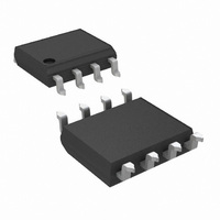
CLC007BMX/NOPB National Semiconductor, CLC007BMX/NOPB Datasheet - Page 4

CLC007BMX/NOPB
Manufacturer Part Number
CLC007BMX/NOPB
Description
IC CABLE DVR DGTL DUAL 8-SOIC
Manufacturer
National Semiconductor
Series
CLCr
Type
Driverr
Datasheet
1.CLC007BMNOPB.pdf
(10 pages)
Specifications of CLC007BMX/NOPB
Number Of Drivers/receivers
1/0
Voltage - Supply
4.5 V ~ 5.5 V
Mounting Type
Surface Mount
Package / Case
8-SOIC (3.9mm Width)
For Use With
SD007EVK - BOARD EVALUATION CLC007
Lead Free Status / RoHS Status
Lead free / RoHS Compliant
Protocol
-
Other names
CLC007BMX
www.national.com
Operation
INPUT INTERFACING
The CLC007 has high impedance, emitter-follower buffered,
differential inputs. Single-ended signals may also be input.
Transmission lines supplying input signals must be properly
terminated close to the CLC007. Either A.C. or D.C. coupling
as in Figure 2 or Figure 3 may be used. Figures 2, 4 and
ECL, 50Ω, 5V, V
ECL, 50Ω, 5.2V, V
ECL, 75Ω, 5V, V
ECL, 75Ω, 5.2V, V
800 mV
800 mV
800 mV
P-P
P-P
P-P
, 50Ω, 5V, V
, 75Ω, 5V, V
, 2.2 KΩ, 5V, V
T
T
=2V
=2V
T
T
=2V
=2V
T
T
=1.6V
=1.6V
T
Load Type
=1.6V
FIGURE 2. AC Coupled Input
FIGURE 1. Input Stage
4
Figure 5 show how Thevenin-equivalent resistor networks are
used to provide input termination and biasing. The input D.C.
common-mode voltage range is 0.8V to 2.5V below the pos-
itive power supply (V
kept within the specified common-mode range. For an
800 mV
1.2V to 2.1V below the positive supply.
Resistor to V
P-P
10008504
3240Ω
82.5Ω
80.6Ω
75.0Ω
124Ω
121Ω
110Ω
input signal, typical input bias levels range from
CC
(R1)
CC
). Input signals plus bias should be
10008505
Resistor to V
6810Ω
124Ω
133Ω
187Ω
196Ω
154Ω
232Ω
EE
(R2)


