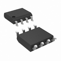
CLC007BMX/NOPB National Semiconductor, CLC007BMX/NOPB Datasheet - Page 7

CLC007BMX/NOPB
Manufacturer Part Number
CLC007BMX/NOPB
Description
IC CABLE DVR DGTL DUAL 8-SOIC
Manufacturer
National Semiconductor
Series
CLCr
Type
Driverr
Datasheet
1.CLC007BMNOPB.pdf
(10 pages)
Specifications of CLC007BMX/NOPB
Number Of Drivers/receivers
1/0
Voltage - Supply
4.5 V ~ 5.5 V
Mounting Type
Surface Mount
Package / Case
8-SOIC (3.9mm Width)
For Use With
SD007EVK - BOARD EVALUATION CLC007
Lead Free Status / RoHS Status
Lead free / RoHS Compliant
Protocol
-
Other names
CLC007BMX
OUTPUT RISE AND FALL TIMES
Output load capacitance can significantly affect output rise
and fall times. The effect of load capacitance, stray or other-
wise, may be reduced by placing the output back-match
PCB Layout Recommendations
Printed circuit board layout affects the performance of the
CLC007. The following guidelines will aid in achieving satis-
factory device performance.
•
•
•
Use a ground plane or power/ground plane sandwich
design for optimum performance.
Bypass device power with a 0.01 µF monolithic ceramic
capacitor in parallel with a 6.8 µF tantalum electrolytic
capacitor located no more than 0.1” (2.5 mm) from the
device power pins.
Provide short, symmetrical ground return paths for:
FIGURE 7. Differential Input DC Coupled Output
FIGURE 8. Rise Time vs C
7
resistor close to the output pin and by minimizing all intercon-
necting trace lengths. Figure 8 shows the effect on risetime
of parallel load capacitance across a 150Ω load.
•
— inputs,
— supply bypass capacitors and
— the output load.
Provide short, grounded guard traces located
— under the centerline of the package,
— 0.1” (2.5 mm) from the package pins
— on both top and bottom of the board with connecting
vias.
L
10008511
10008510
www.national.com


