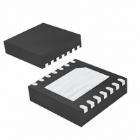
MAX13342EETD+T Maxim Integrated Products, MAX13342EETD+T Datasheet - Page 2

MAX13342EETD+T
Manufacturer Part Number
MAX13342EETD+T
Description
IC TXRX USB FS 3WIRE 14-TDFN
Manufacturer
Maxim Integrated Products
Type
Transceiverr
Datasheet
1.MAX13345EETDT.pdf
(18 pages)
Specifications of MAX13342EETD+T
Number Of Drivers/receivers
1/1
Protocol
USB 2.0
Voltage - Supply
2.3 V ~ 3.6 V
Mounting Type
Surface Mount
Package / Case
14-TDFN Exposed Pad
Lead Free Status / RoHS Status
Lead free / RoHS Compliant
ABSOLUTE MAXIMUM RATINGS
(All voltages refer to GND unless otherwise noted.)
Supply Voltage (V
System Supply Voltage (V
Output of Internal Regulator (V
Input Voltage (D+, D-) ..............................................-0.3V to +6V
SUS, BD ........................................................-0.3V to (V
ENUM, SE0, DAT ..........................................-0.3V to (V
Short-Circuit Current to V
Maximum Continuous Current (all other pins) ..................±15mA
3-Wire Interface Full-Speed USB Transceivers
With/Without Internal Series Resistors
ELECTRICAL CHARACTERISTICS
(V
+2.5V, T
Stresses beyond those listed under “Absolute Maximum Ratings” may cause permanent damage to the device. These are stress ratings only, and functional
operation of the device at these or any other conditions beyond those indicated in the operational sections of the specifications is not implied. Exposure to
absolute maximum rating conditions for extended periods may affect device reliability.
2
SUPPLY INPUTS (V
V
V
Reg ul ated S up p l y- V ol tag e Outp ut
Operating V
Operating V
Full-Speed Idle and SE0 Supply
Current
Static V
Suspend Supply Current
Disable-Mode Supply Current
Sharing-Mode V
D+/D- Supply Current
V
Threshold
V
Hysteresis
V
BUS
BUS
L
BUS
BUS
L
Input Range
Power-Supply Threshold
_______________________________________________________________________________________
= +4.0V to +5.5V, V
Input Range
Power-Supply Detection
Power-Supply Detection
A
L
Supply Current
= +25°C.) (Note 1)
PARAMETER
BUS
L
Supply Current
L
Supply Current
BUS
Supply Current I
) .............................................-0.3V to +6V
BUS
BUS
L
, V
) .....................................-0.3V to +6V
L
TRM
= +2.3V to +3.6V, T
or GND (D+, D-) ..............±150mA
TRM
, V
) .........-0.3V to (V
L
I
VBUS(SUSP)
)
I
I
V L( S H ARIN G)
V
VBUS(IDLE)
I
V
VL(STATIC)
SYMBOL
VBUS(DIS)
VBUSHYS
TH_VBUS
V
I
I
V
V
VBUS
D+/D-
TH_VL
I
BUS
V
TRM
VL
L
A
Full-speed transmitting/receiving at
12Mbps, C
Ful l - sp eed tr ansm i tti ng /r ecei vi ng at 12M b p s,
C
Full-speed idle, V
SE0: V
Full-speed idle, SE0 or suspend mode
SE0 = DAT= open;
SUS = OE = high
V
V
SE0 = DAT = low or high, SUS = high
V
V
= T
L
BUS
BUS
L
BUS
L
= GND or open
> 2.3V
= 15pF receiver outputs, V
MIN
L
L
= GND or open, OE = low,
= GND or open
+ 0.3V)
+ 0.3V)
+ 0.3V)
D-
to T
<0.3V, V
L
MAX
= 50pF on D+ and D-
CONDITIONS
, unless otherwise noted. Typical values are at V
D+
D+
Continuous Power Dissipation (T
Operating Temperature Range ...........................-40°C to +85°C
Junction Temperature ......................................................+150°C
Storage Temperature Range .............................-65°C to +150°C
Bump Soldering ...............................................................+235°C
Lead Soldering (10s) ...................................................... +300°C
>2.7V, V
<0.3
14-Pin TDFN (derate 18.5mW/°C above +70°C) .......1482mW
4mm x 3mm UCSP
(derate 6.5mW/°C above +70°C) ..............................518mW
D-
L
= 2.5V
<0.3V
MIN
4.0
2.3
3.0
0.8
A
= +70°C)
TYP
100
850
3.3
1.5
30
BUS
MAX
500
500
5.5
3.6
3.6
3.6
10
10
45
25
20
5
= +5.0V, V
UNITS
mA
mA
mV
mV
µA
µA
µA
µA
µA
µA
V
V
V
V
L
=


