MAX9111EKA+T Maxim Integrated Products, MAX9111EKA+T Datasheet
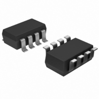
IC RCVR SNGL LVDS SOT23-8

MAX9111EKA+T

Manufacturer Part Number
MAX9111EKA+T
Description
IC RCVR SNGL LVDS SOT23-8
Manufacturer
Maxim Integrated Products
Type
Receiverr
Datasheets

Specifications of MAX9111EKA+T

Number Of Drivers/receivers
0/1
Protocol
LVDS
Voltage - Supply
3 V ~ 3.6 V
Mounting Type
Surface Mount
Package / Case
SOT-23-8
Logic Family
MAX9111
Logic Type
LVDS Line Receiver
Supply Voltage (max)
4 V
Supply Voltage (min)
- 0.3 V
Maximum Operating Temperature
+ 85 C
Mounting Style
SMD/SMT
Data Rate
500 Mbps
Maximum Power Dissipation
714 mW
Minimum Operating Temperature
- 40 C
Output Voltage
+/- 0.3 V
Propagation Delay Time
1.77 ns
Supply Current
4.2 mA
Lead Free Status / RoHS Status
Lead free / RoHS Compliant
The MAX9111/MAX9113 single/dual low-voltage differen-
tial signaling (LVDS) receivers are designed for high-
speed applications requiring minimum power
consumption, space, and noise. Both devices support
switching rates exceeding 500Mbps while operating from
a single +3.3V supply, and feature ultra-low 300ps (max)
pulse skew required for high-resolution imaging applica-
tions such as laser printers and digital copiers.
The MAX9111 is a single LVDS receiver, and the
MAX9113 is a dual LVDS receiver.
Both devices conform to the EIA/TIA-644 LVDS standard
and convert LVDS to LVTTL/CMOS-compatible outputs.
A fail-safe feature sets the outputs high when the inputs
are undriven and open, terminated, or shorted. The
MAX9111/MAX9113 are available in space-saving 8-pin
SOT23 and SO packages. Refer to the MAX9110/
MAX9112 data sheet for single/dual LVDS line drivers.
19-1803; Rev 3; 3/09
Laser Printers
Digital Copiers
Cellular Phone
Base Stations
Telecom Switching
Equipment
For pricing, delivery, and ordering information, please contact Maxim Direct at 1-888-629-4642,
or visit Maxim's website at www.maxim-ic.com.
________________________Applications
N.C.
N.C.
IN+
IN-
1
2
4
3
MAX9111
SO
________________________________________________________________ Maxim Integrated Products
General Description
Single/Dual LVDS Line Receivers with
6
8
7
5
V
OUT
N.C.
GND
CC
Network Switches/Routers
LCD Displays
Backplane Interconnect
Clock Distribution
GND
V
OUT
N.C.
CC
Pin Configurations/Functional Diagrams/Truth Table
100Ω PARALLEL TERMINATION (UNDRIVEN)
1
2
4
3
Ultra-Low Pulse Skew in SOT23
MAX9111
MAX9111
SOT23
(IN_+) - (IN_-)
≥ -100mV
≥ 100mV
SHORT
OPEN
6
8
7
5
IN-
IN+
N.C.
N.C.
IN1+
IN2+
IN1-
IN2-
o Low 300ps (max) Pulse Skew for High-Resolution
o Space-Saving 8-Pin SOT23 and SO Packages
o Pin-Compatible Upgrades to DS90LV018A and
o Guaranteed 500Mbps Data Rate
o Low 29mW Power Dissipation at 3.3V
o Conform to EIA/TIA-644 Standard
o Single +3.3V Supply
o Flow-Through Pinout Simplifies PCB Layout
o Fail-Safe Circuit Sets Output High for Undriven
o High-Impedance LVDS Inputs when Powered Off
/V denotes an automotive qualified part.
+ Denotes a lead(Pb)-free/RoHS-compliant package.
Typical Operating Circuit appears at end of data sheet.
MAX9111EKA
MAX9111ESA
MAX9113EKA
MAX9113ESA
MAX9113ASA/V+
Imaging and High-Speed Interconnect
DS90LV028A (SO Packages Only)
Inputs
1
2
4
3
OUT_
H
L
H
H
H
PART
MAX9113
SO
H = LOGIC LEVEL HIGH
L = LOGIC LEVEL LOW
6
8
7
5
-40°C to +85°C
-40°C to +85°C
-40°C to +85°C
-40°C to +85°C
-40°C to +125°C 8 SO
V
OUT1
OUT2
GND
CC
Ordering Information
RANGE
TEMP
OUT1
OUT2
GND
V
CC
1
2
4
3
MAX9113
SOT23
PIN-
PACKAGE
8 SOT23
8 SO
8 SOT23
8 SO
Features
7
6
5
8
MARK
IN1-
IN1+
IN2+
IN2-
AAED
AAEE
TOP
1

Related parts for MAX9111EKA+T

MAX9111EKA+T Summary of contents

Page 1

... N. GND N.C. SO ________________________________________________________________ Maxim Integrated Products For pricing, delivery, and ordering information, please contact Maxim Direct at 1-888-629-4642, or visit Maxim's website at www.maxim-ic.com. Ultra-Low Pulse Skew in SOT23 o Low 300ps (max) Pulse Skew for High-Resolution Imaging and High-Speed Interconnect o Space-Saving 8-Pin SOT23 and SO Packages ...

Page 2

Single/Dual LVDS Line Receivers with Ultra-Low Pulse Skew in SOT23 ABSOLUTE MAXIMUM RATINGS V to GND ..............................................................-0.3V to +4V CC IN_ _ to GND .........................................................-0.3V to +3.9V OUT_ _ to GND...........................................-0. ESD Protection All Pins (Human Body Model, ...

Page 3

Single/Dual LVDS Line Receivers with SWITCHING CHARACTERISTICS (V = +3.0V to +3.6V MIN MAX PARAMETER SYMBOL Differential Propagation Delay High to Low Differential Propagation Delay Low to High Differential Pulse Skew |t - ...

Page 4

Single/Dual LVDS Line Receivers with Ultra-Low Pulse Skew in SOT23 Figure 1. Receiver Propagation Delay and Transition Time Test Circuit IN_- IN_+ OUT_ Figure 2. Receiver Propagation Delay and Transition Time Waveforms 4 _______________________________________________________________________________________ IN_+ GENERATOR IN_ 50Ω ...

Page 5

Single/Dual LVDS Line Receivers with (V = 3.3V 200mV 1.2V unless otherwise specified.) OUTPUT HIGH VOLTAGE vs. SUPPLY VOLTAGE 3 4mA 3.6 OUT_ 3.5 3.4 3.3 3.2 3.1 3.0 ...

Page 6

Single/Dual LVDS Line Receivers with Ultra-Low Pulse Skew in SOT23 (V = 3.3V 200mV 1.2V unless otherwise specified.) DIFFERENTIAL PULSE SKEW vs. TEMPERATURE 250 200 150 100 50 0 -40 -15 ...

Page 7

Single/Dual LVDS Line Receivers with PIN MAX9111 MAX9113 SOT23-8 SO-8 SOT23 — — 5 — — — — ...

Page 8

Single/Dual LVDS Line Receivers with Ultra-Low Pulse Skew in SOT23 1MΩ 1500Ω DISCHARGE CHARGE-CURRENT RESISTANCE LIMIT RESISTOR HIGH STORAGE VOLTAGE 100pF CAPACITOR DC SOURCE Figure 3a. Human Body ESD Test Modules __________ Applications Information ...

Page 9

Single/Dual LVDS Line Receivers with DIN_ Chip Information PROCESS: CMOS _______________________________________________________________________________________ Ultra-Low Pulse Skew in SOT23 +3.3V 0.001μF 0.1μF DRIVER R = 100Ω T LVDS MAX9111 MAX9110 MAX9113 MAX9112 For the latest package outline information and land patterns ...

Page 10

... Maxim cannot assume responsibility for use of any circuitry other than circuitry entirely embodied in a Maxim product. No circuit patent licenses are implied. Maxim reserves the right to change the circuitry and specifications without notice at any time. 10 ____________________Maxim Integrated Products, 120 San Gabriel Drive, Sunnyvale, CA 94086 408-737-7600 © 2009 Maxim Integrated Products DESCRIPTION Maxim is a registered trademark of Maxim Integrated Products, Inc ...

Related keywords