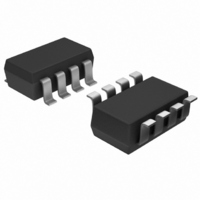
MAX9111EKA+T Maxim Integrated Products, MAX9111EKA+T Datasheet - Page 7

MAX9111EKA+T
Manufacturer Part Number
MAX9111EKA+T
Description
IC RCVR SNGL LVDS SOT23-8
Manufacturer
Maxim Integrated Products
Type
Receiverr
Specifications of MAX9111EKA+T
Number Of Drivers/receivers
0/1
Protocol
LVDS
Voltage - Supply
3 V ~ 3.6 V
Mounting Type
Surface Mount
Package / Case
SOT-23-8
Logic Family
MAX9111
Logic Type
LVDS Line Receiver
Supply Voltage (max)
4 V
Supply Voltage (min)
- 0.3 V
Maximum Operating Temperature
+ 85 C
Mounting Style
SMD/SMT
Data Rate
500 Mbps
Maximum Power Dissipation
714 mW
Minimum Operating Temperature
- 40 C
Output Voltage
+/- 0.3 V
Propagation Delay Time
1.77 ns
Supply Current
4.2 mA
Lead Free Status / RoHS Status
Lead free / RoHS Compliant
The MAX9111/MAX9113 feature LVDS inputs for inter-
facing high-speed digital circuitry. The LVDS interface
standard is a signaling method intended for point-to-
point communication over a controlled impedance
media, as defined by the ANSI/EIA/TIA-644 standards.
The technology uses low-voltage signals to achieve fast
transition times, minimize power dissipation, and noise
immunity. Receivers such as the MAX9111/MAX9113
convert LVDS signals to CMOS/LVTTL signals at rates
in excess of 500Mbps. The devices are capable of
detecting differential signals as low as 100mV and as
high as 1V within a 0V to 2.4V input voltage range . The
LVDS standard specifies an input voltage range of 0 to
2.4V referenced to ground.
The fail-safe feature sets the output to a high state
when the inputs are undriven and open, terminated, or
shorted. When using one channel in the MAX9113,
leave the unused channel open. The fail-safe feature is
not guaranteed to be operational above +85°C.
_______________Detailed Description
SOT23-8
4, 5, 6
—
—
—
1
2
8
7
3
MAX9111
3, 4, 6
SO-8
—
—
—
8
5
1
2
7
_______________________________________________________________________________________
PIN
SOT23-8
Single/Dual LVDS Line Receivers with
—
1
2
8
7
5
6
3
4
MAX9113
SO-8
—
8
5
1
2
4
3
7
6
Ultra-Low Pulse Skew in SOT23
LVDS Inputs
Fail-Safe
OUT/OUT1
IN+/IN1+
IN-/IN1-
NAME
OUT2
GND
IN2+
N.C.
V
IN2-
CC
Power Supply
Ground
No Connection. Not internally connected.
Receiver Inverting Differential Input
Receiver Noninverting Differential Input
Receiver Inverting Differential Input
Receiver Noninverting Differential Input
Receiver Output
Receiver Output
As with all Maxim devices, ESD-protection structures are
incorporated on all pins to protect against electrostatic
discharges encountered during handling and assembly.
The receiver inputs of the MAX9111/MAX9113 have extra
protection against static electricity. Maxim’s engineers
have developed state-of-the-art structures to protect
these pins against ESD of ±11kV without damage. The
ESD structures withstand high ESD in all states: normal
operation, shutdown, and powered down.
ESD protection can be tested in various ways; the
receiver inputs of this product family are characterized
for protection to the limit of ±11kV using the Human
Body Model.
Figure 3a shows the Human Body Model, and Figure
3b shows the current waveform it generates when dis-
charged into a low impedance. This model consists of a
100pF capacitor charged to the ESD voltage of interest,
which is then discharged into the test device through a
1.5kΩ resistor.
FUNCTION
Pin Description
Human Body Model
ESD Protection
7


