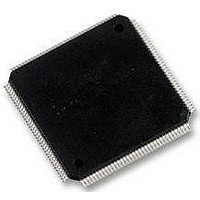
MK20DN512ZVLQ10 Freescale Semiconductor, MK20DN512ZVLQ10 Datasheet - Page 21

MK20DN512ZVLQ10
Manufacturer Part Number
MK20DN512ZVLQ10
Description
KINETIS 512K USB
Manufacturer
Freescale Semiconductor
Datasheet
1.MK20DN512ZVLQ10.pdf
(74 pages)
Specifications of MK20DN512ZVLQ10
Processor Series
K20
Core
ARM Cortex M4
Data Bus Width
16 bit
Program Memory Type
Flash
Program Memory Size
512 KB
Data Ram Size
128 KB
Interface Type
USB, CAN, SPI, I2C, UART
Maximum Clock Frequency
100 MHz
Number Of Programmable I/os
2
Number Of Timers
2
Operating Supply Voltage
1.71 V to 3.6 V
Maximum Operating Temperature
+ 105 C
Mounting Style
SMD/SMT
Package / Case
LQFP-144
Operating Temperature Range
- 40 C to + 105 C
Processor To Be Evaluated
MK20DN512ZVLQ10
Supply Current (max)
185 mA
Lead Free Status / Rohs Status
No
Available stocks
Company
Part Number
Manufacturer
Quantity
Price
Company:
Part Number:
MK20DN512ZVLQ10
Manufacturer:
Freescale Semiconductor
Quantity:
10 000
Company:
Part Number:
MK20DN512ZVLQ10R
Manufacturer:
Freescale Semiconductor
Quantity:
10 000
www.DataSheet.co.kr
5.3.2 General switching specifications
These general purpose specifications apply to all signals configured for GPIO, UART,
CAN, CMT, and I
1. The greater synchronous and asynchronous timing must be met.
2. This is the shortest pulse that is guaranteed to be recognized.
3. 75pF load
4. 15pF load
5.4 Thermal specifications
Freescale Semiconductor, Inc.
Symbol
GPIO pin interrupt pulse width (digital glitch filter
disabled) — Synchronous path
GPIO pin interrupt pulse width (digital glitch filter
disabled, analog filter enabled) — Asynchronous path
GPIO pin interrupt pulse width (digital glitch filter
disabled, analog filter disabled) — Asynchronous path
External reset pulse width (digital glitch filter disabled)
Mode select (EZP_CS) hold time after reset
deassertion
Port rise and fall time (high drive strength)
Port rise and fall time (low drive strength)
Description
• Slew disabled
• Slew enabled
• Slew disabled
• Slew enabled
• 1.71 ≤ V
• 2.7 ≤ V
• 1.71 ≤ V
• 2.7 ≤ V
• 1.71 ≤ V
• 2.7 ≤ V
• 1.71 ≤ V
• 2.7 ≤ V
2
C signals.
K20 Sub-Family Data Sheet Data Sheet, Rev. 6, 9/2011.
Table 10. General switching specifications
DD
DD
DD
DD
DD
DD
DD
DD
≤ 3.6V
≤ 3.6V
≤ 3.6V
≤ 3.6V
≤ 2.7V
≤ 2.7V
≤ 2.7V
≤ 2.7V
Min.
100
100
1.5
16
—
—
—
—
—
—
—
—
2
Max.
12
36
24
12
36
24
—
—
—
—
—
6
6
Bus clock
Bus clock
cycles
cycles
Unit
ns
ns
ns
ns
ns
ns
ns
ns
ns
ns
ns
Notes
General
1
2
2
2
3
4
21
Datasheet pdf - http://www.DataSheet4U.net/


