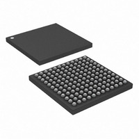
DS26522GN+ Maxim Integrated Products, DS26522GN+ Datasheet - Page 25

DS26522GN+
Manufacturer Part Number
DS26522GN+
Description
IC TXRX T1/E1/J1 DUAL 144CSBGA
Manufacturer
Maxim Integrated Products
Type
Transceiverr
Specifications of DS26522GN+
Number Of Drivers/receivers
2/2
Protocol
RS232
Voltage - Supply
3.14 V ~ 3.47 V
Mounting Type
Surface Mount
Package / Case
144-CSBGA
Lead Free Status / RoHS Status
Lead free / RoHS Compliant
- Current page: 25 of 258
- Download datasheet (2Mb)
8.
8.1
8.1.1 Parallel Port Mode
Parallel port control of the DS26522 is accomplished through the 26 hardware pins of the microprocessor port. The
8-bit parallel data bus can be configured for Intel or Motorola modes of operation with the bus type select (BTS)
pin. When the BTS pin is a logic 0, bus timing is in Intel mode, as shown in
BTS pin is a logic 1, bus timing is in Motorola mode, as shown in
is mapped through the use of 10 address lines, A[8:0] and A12. Multiplexed mode is not supported on the
processor interface.
8.1.2 SPI Serial Port Mode
The external processor bus can be configured to operate in SPI serial bus mode. See Section
timing diagrams.
When SPI_SEL = 1, SPI bus mode is implemented using four signals: clock (SPI_SCLK), master-out/slave-in data
(SPI_MOSI), master-in/slave-out data (SPI_MISO), and chip select (CSBn). Clock polarity and phase can be set by
the D[7]/SPI_CPOL and D[6]/SPI_CPHA pins.
The order of the address and data bits in the serial stream is selectable using the D[5]/SPI_SWAP pin. The R/W bit
is always first and B bit is always last in the initial control word and are not affected by the D[5]/SPI_SWAP pin
setting.
The chip-select bar (CSBn) pin must be brought to a logic-low level to gain read and write access to the
microprocessor port. With Intel timing selected, the read-data bar (RDB) and write-read bar (WRB) pins are used to
indicate read and write operations and latch data through the interface. With Motorola timing selected, the read-
write bar (RWB) pin is used to indicate read and write operations while the data-strobe bar (DSB) pin is used to
latch data through the interface.
The interrupt output pin (INTB) is an open-drain output that asserts a logic-low level upon a number of software
maskable interrupt conditions. This pin is normally connected to the microprocessor interrupt input.
8.1.3 SPI Functional Timing Diagrams
Note: The transmit and receive order of the address and data bits are selected by the D[5]/SPI_SWAP pin. The
R/W (read/write) MSB bit position and B (burst) LSB bit position are not affected by the D[5]/SPI_SWAP pin setting.
8.1.3.1 SPI Transmission Format and CPHA Polarity
When CPHA = 0, CSBn may be deasserted between accesses. An access is defined as one or two control bytes
followed by a data byte. CSBn cannot be deasserted between the control bytes, or between the last control byte
and the data byte. When CPHA = 0, CSBn may also remain asserted between accesses. If it remains asserted and
the BURST bit is set, no additional control bytes are expected after the first control byte(s) and data are transferred.
If the BURST bit is set, the address will be incremented for each additional byte of data transferred until CSBn is
deasserted. If CSBn remains asserted and the BURST bit is not set, a control byte(s) is expected following the data
byte, and the address for the next access will be received from that. Anytime CSBn is deasserted, the BURST
access is terminated.
When CPHA = 1, CSBn may remain asserted for more than one access without being toggled high and then low
again between accesses. If the BURST bit is set, the address should increment and no additional control bytes are
expected. If the BURST bit is not set, each data byte will be followed by the control byte(s) for the next access.
Additionally, CSBn may also be deasserted between accesses when CPHA =1. In the case, any BURST access is
terminated, and the next byte received when CSBn is reasserted will be a control byte.
The following diagrams describe the functionality of the SPI port for the four combinations of SPI_CPOL and
SPI_CPHA. They indicate the clock edge that samples the data and the level of the clock during no-transfer events
(high or low). Since the SPI port of the DS26522 acts as a slave device, the master device provides the clock. The
Microprocessor Interface
FUNCTIONAL DESCRIPTION
25 of 258
Figure 12-3
Figure 12-1
DS26522 Dual T1/E1/J1 Transceiver
and
Figure
and
12-4. The address space
Figure
8.1.3
12-2. When the
for detailed
Related parts for DS26522GN+
Image
Part Number
Description
Manufacturer
Datasheet
Request
R

Part Number:
Description:
Ds26522 Dual T1/e1/j1 Transceiver
Manufacturer:
Maxim Integrated Products, Inc.
Datasheet:

Part Number:
Description:
power light source LUXEON® Collimator
Manufacturer:
LUMILEDS [Lumileds Lighting Company]
Datasheet:

Part Number:
Description:
MAX7528KCWPMaxim Integrated Products [CMOS Dual 8-Bit Buffered Multiplying DACs]
Manufacturer:
Maxim Integrated Products
Datasheet:

Part Number:
Description:
Single +5V, fully integrated, 1.25Gbps laser diode driver.
Manufacturer:
Maxim Integrated Products
Datasheet:

Part Number:
Description:
Single +5V, fully integrated, 155Mbps laser diode driver.
Manufacturer:
Maxim Integrated Products
Datasheet:

Part Number:
Description:
VRD11/VRD10, K8 Rev F 2/3/4-Phase PWM Controllers with Integrated Dual MOSFET Drivers
Manufacturer:
Maxim Integrated Products
Datasheet:

Part Number:
Description:
Highly Integrated Level 2 SMBus Battery Chargers
Manufacturer:
Maxim Integrated Products
Datasheet:

Part Number:
Description:
Current Monitor and Accumulator with Integrated Sense Resistor; ; Temperature Range: -40°C to +85°C
Manufacturer:
Maxim Integrated Products

Part Number:
Description:
TSSOP 14/A°/RS-485 Transceivers with Integrated 100O/120O Termination Resis
Manufacturer:
Maxim Integrated Products

Part Number:
Description:
TSSOP 14/A°/RS-485 Transceivers with Integrated 100O/120O Termination Resis
Manufacturer:
Maxim Integrated Products

Part Number:
Description:
QFN 16/A°/AC-DC and DC-DC Peak-Current-Mode Converters with Integrated Step
Manufacturer:
Maxim Integrated Products

Part Number:
Description:
TDFN/A/65V, 1A, 600KHZ, SYNCHRONOUS STEP-DOWN REGULATOR WITH INTEGRATED SWI
Manufacturer:
Maxim Integrated Products

Part Number:
Description:
Integrated Temperature Controller f
Manufacturer:
Maxim Integrated Products

Part Number:
Description:
SOT23-6/I°/45MHz to 650MHz, Integrated IF VCOs with Differential Output
Manufacturer:
Maxim Integrated Products


