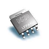
PSMN1R5-30YLC,115 NXP Semiconductors, PSMN1R5-30YLC,115 Datasheet - Page 9

PSMN1R5-30YLC,115
Manufacturer Part Number
PSMN1R5-30YLC,115
Description
MOSFET Power N-Ch 30V 1.55mOhms
Manufacturer
NXP Semiconductors
Series
-r
Datasheet
1.PSMN1R5-30YLC115.pdf
(15 pages)
Specifications of PSMN1R5-30YLC,115
Transistor Polarity
N-Channel
Resistance Drain-source Rds (on)
1.55 mOhms
Drain-source Breakdown Voltage
30 V
Gate-source Breakdown Voltage
20 V
Continuous Drain Current
100 A
Power Dissipation
179 W
Maximum Operating Temperature
+ 175 C
Mounting Style
SMD/SMT
Package / Case
LFPAK
Gate Charge Qg
65 nC
Minimum Operating Temperature
- 55 C
Fet Type
MOSFET N-Channel, Metal Oxide
Fet Feature
Logic Level Gate
Rds On (max) @ Id, Vgs
1.55 mOhm @ 25A, 10V
Drain To Source Voltage (vdss)
30V
Current - Continuous Drain (id) @ 25° C
100A
Vgs(th) (max) @ Id
1.95V @ 1mA
Gate Charge (qg) @ Vgs
65nC @ 10V
Input Capacitance (ciss) @ Vds
4044pF @ 15V
Power - Max
179W
Mounting Type
Surface Mount
Lead Free Status / Rohs Status
Details
Other names
934065188115
NXP Semiconductors
PSMN1R5-30YLC
Product data sheet
Fig 12. Drain-source on-state resistance as a function
Fig 14. Gate charge waveform definitions
(mΩ)
R
DS on
8
6
4
2
0
of drain current; typical values
0
V
V
V
V
GS(pl)
DS
GS(th)
GS
Q
25
GS1
I
Q
D
GS
Q
GS2
50
Q
G(tot)
2.6
Q
GD
75
N-channel 30 V 1.55mΩ logic level MOSFET in LFPAK using NextPower
V
GS
4.5
All information provided in this document is subject to legal disclaimers.
003a a f 649
003aaa508
(V) = 2.8
I
D
(A)
3.0
3.5
10
100
Rev. 2 — 17 May 2011
Fig 13. Normalized drain-source on-state resistance
Fig 15. Gate-source voltage as a function of gate
V
(V)
a
GS
1.5
0.5
10
2
1
0
8
6
4
2
0
-60
factor as a function of junction temperature
charge; typical values
0
20
0
PSMN1R5-30YLC
60
40
V
DS
15V
= 6V
24V
10V
120
60
© NXP B.V. 2011. All rights reserved.
V
003a a f 656
GS
Q
003a a f 650
T
G
j
=4.5V
(°C)
(nC)
180
80
9 of 15


