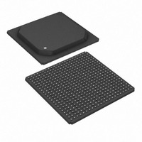
DS32508N+ Maxim Integrated Products, DS32508N+ Datasheet - Page 22

DS32508N+
Manufacturer Part Number
DS32508N+
Description
IC LIU DS3/E3/STS-1 484-BGA
Manufacturer
Maxim Integrated Products
Type
Line Interface Units (LIUs)r
Datasheet
1.DS32506N.pdf
(130 pages)
Specifications of DS32508N+
Protocol
IEEE 1149.1
Voltage - Supply
1.8V, 3.3V
Mounting Type
Surface Mount
Package / Case
484-BGA
Lead Free Status / RoHS Status
Lead free / RoHS Compliant
Number Of Drivers/receivers
-
- Current page: 22 of 130
- Download datasheet (2Mb)
Table 7-7. SPI Serial Interface Pin Descriptions
Table 7-8. CLAD Pin Descriptions
CLADBYP
REFCLK
GPIOAn
GPIOBn
NAME
NAME
CLKC
CLKD
CPHA
CPOL
CLKA
CLKB
SCLK
SDO
SDI
INT
CS
TYPE
TYPE
I/Opd
I/Opd
I/O
I/O
I/O
Oz
O
O
I
I
I
I
I
I
I
Chip Select (Active Low). This pin must be asserted to read or write internal registers.
See Section 8.9.
Serial Clock. SCLK is always driven by the SPI bus master. See Section 8.9.
Serial Data Input. The SPI bus master transmits data to the device on this pin.
See Section 8.9.
Serial Data Output. The device transmits data to the SPI bus master on this pin.
See Section 8.9.
Clock Phase. See Section 8.9.
0 = Data is latched on the leading edge of the SCLK pulse
1 = Data is latched on the trailing edge of the SCLK pulse
Clock Polarity. See Section 8.9.
0 = SCLK is normally low and pulses high during bus transactions
1 = SCLK is normally high and pulses low during bus transactions
Interrupt Output (Active Low, Open Drain).
See
General-Purpose I/O A. See
General-Purpose I/O B. See
Reference Clock. The signal on this pin is the input reference clock to the CLAD and
must be transmission quality (±20ppm, low jitter). In hardware mode, REFCLK must be
19.44MHz. In bus interface modes, REFCLK can be any of several frequencies. See
Section 8.7.1.
Clock A—DS3 44.736MHz. When the CLAD is bypassed, a transmission-quality DS3
clock (44.736MHz ±20ppm, low jitter) must be connected to this pin if any of the LIUs are
to operate in DS3 mode. When the CLAD is enabled this pin can be configured to output
the DS3 clock synthesized by PLL-A. See Section 8.7.1.
Clock B—E3 34.368MHz. When the CLAD is bypassed, a transmission-quality E3 clock
(34.368MHz ±20ppm, low jitter) must be connected to this pin if any of the LIUs are to
operate in E3 mode. When the CLAD is enabled, this pin can be configured to output the
E3 clock synthesized by PLL-B. See Section 8.7.1.
Clock C—STS-1 51.84MHz. When the CLAD is bypassed, a transmission-quality STS-1
clock (51.84MHz ±20ppm, low jitter) must be connected to this pin if any of the LIUs are
to operate in STS-1 mode. When the CLAD is enabled, this pin can be configured to
output the STS-1 clock synthesized by PLL-C. See Section 8.7.1.
Clock D—Telecom Bus 77.76MHz or 19.44MHz. When the CLAD is bypassed, this pin
is driven low. When the CLAD is enabled this pin can output a 77.76MHz or 19.44MHz
clock synthesized by PLL-D. See Section 8.7.1.
CLAD Bypass Control. This pin controls whether the CLAD is used or bypassed. When
a microprocessor interface is enabled
allow use of the GLOBAL.CR2:CLAD[6:0] field to control the CLAD. See Section 8.7.1.
0 = Synthesize the DS3, E3, and STS-1 clocks from the clock on the
1 = Source the DS3, E3, and STS-1 clocks from the CLKA,
INT
pin description in
Table
22 of 130
GPIOAn
GPIOBn
7-6.
pin description in
pin description in
(IFSEL
FUNCTION
FUNCTION
≠ 000), CLADBYP should be wired low to
Table
Table
CLKB
7-6.
7-6.
DS32506/DS32508/DS32512
and
REFCLK
CLKC
pins.
pin.
Related parts for DS32508N+
Image
Part Number
Description
Manufacturer
Datasheet
Request
R

Part Number:
Description:
MAX7528KCWPMaxim Integrated Products [CMOS Dual 8-Bit Buffered Multiplying DACs]
Manufacturer:
Maxim Integrated Products
Datasheet:

Part Number:
Description:
Single +5V, fully integrated, 1.25Gbps laser diode driver.
Manufacturer:
Maxim Integrated Products
Datasheet:

Part Number:
Description:
Single +5V, fully integrated, 155Mbps laser diode driver.
Manufacturer:
Maxim Integrated Products
Datasheet:

Part Number:
Description:
VRD11/VRD10, K8 Rev F 2/3/4-Phase PWM Controllers with Integrated Dual MOSFET Drivers
Manufacturer:
Maxim Integrated Products
Datasheet:

Part Number:
Description:
Highly Integrated Level 2 SMBus Battery Chargers
Manufacturer:
Maxim Integrated Products
Datasheet:

Part Number:
Description:
Current Monitor and Accumulator with Integrated Sense Resistor; ; Temperature Range: -40°C to +85°C
Manufacturer:
Maxim Integrated Products

Part Number:
Description:
TSSOP 14/A�/RS-485 Transceivers with Integrated 100O/120O Termination Resis
Manufacturer:
Maxim Integrated Products

Part Number:
Description:
TSSOP 14/A�/RS-485 Transceivers with Integrated 100O/120O Termination Resis
Manufacturer:
Maxim Integrated Products

Part Number:
Description:
QFN 16/A�/AC-DC and DC-DC Peak-Current-Mode Converters with Integrated Step
Manufacturer:
Maxim Integrated Products

Part Number:
Description:
TDFN/A/65V, 1A, 600KHZ, SYNCHRONOUS STEP-DOWN REGULATOR WITH INTEGRATED SWI
Manufacturer:
Maxim Integrated Products

Part Number:
Description:
Integrated Temperature Controller f
Manufacturer:
Maxim Integrated Products

Part Number:
Description:
SOT23-6/I�/45MHz to 650MHz, Integrated IF VCOs with Differential Output
Manufacturer:
Maxim Integrated Products

Part Number:
Description:
SOT23-6/I�/45MHz to 650MHz, Integrated IF VCOs with Differential Output
Manufacturer:
Maxim Integrated Products

Part Number:
Description:
EVALUATION KIT/2.4GHZ TO 2.5GHZ 802.11G/B RF TRANSCEIVER WITH INTEGRATED PA
Manufacturer:
Maxim Integrated Products

Part Number:
Description:
QFN/E/DUAL PCIE/SATA HIGH SPEED SWITCH WITH INTEGRATED BIAS RESISTOR
Manufacturer:
Maxim Integrated Products
Datasheet:


