TD62064BF Toshiba, TD62064BF Datasheet - Page 2
TD62064BF
Manufacturer Part Number
TD62064BF
Description
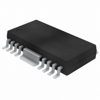
IC DRIVER DARL SINK 4-CH 16-HSOP
Manufacturer
Toshiba
Type
Driverr
Datasheet
1.TD62064BP1G5J.pdf
(11 pages)
Specifications of TD62064BF
Number Of Drivers/receivers
4/0
Protocol
RS232
Voltage - Supply
5V
Mounting Type
Surface Mount
Package / Case
16-HSOP
Lead Free Status / RoHS Status
Contains lead / RoHS non-compliant
Available stocks
Company
Part Number
Manufacturer
Quantity
Price

Part Number:
TD62064BF
Manufacturer:
TOSHIBA/东芝
Quantity:
20 000
Company:
Part Number:
TD62064BFG
Manufacturer:
TOSHIBA
Quantity:
21 009
Part Number:
TD62064BFG
Manufacturer:
TOSHIBA/东芝
Quantity:
20 000


SCHEMATICS
Note :
PRECAUTIONS for USING
(1)
(2)
ABSOLUTE MAXIMUM RATINGS
Output Sustaining Voltage
Parasitic Transistor Output Voltage
Output Current
Input Current
Input Voltage
Clamp Diode Reverse Voltage
Clamp Diode Forward Current
Power Dissipation
Operating Temperature
Storage Temperature
Note 1: Parasitic Transistor (COMMON − GND − OUTPUT) Output Voltage
Note 2: On Glass Epoxy PCB (50 × 50 × 1.6 mm Cu 50%)
Note 3: On Glass Epoxy PCB (60 × 30 × 1.6 mm Cu 30%)
This IC does not include built-in protection circuits for excess current or overvoltage.
If this IC is subjected to excess current or overvoltage, it may be destroyed.
Hence, the utmost care must be taken when systems which incorporate this IC are designed.
Utmost care is necessary in the design of the output line, COMMON and GND line since IC may be destroyed
due to short−circuit between outputs, air contamination fault, or fault by improper grounding.
If a TD62064BP-1/BF is being used to drive an inductive load (such as a motor, solenoid or relay), Toshiba
recommends that the diodes (pins 1 and 8) be connected to the secondary power supply pin so as to absorb the
counter electromotive force generated by the load. Please adhere to the device’s absolute maximum ratings.
Toshiba recommends that zener diodes be connected between the diodes (pins 1 and 8) and the secondary
power supply pin (as the anode) so as to enable rapid absorption of the counter electromotive force. Again,
please adhere to the device’s absolute maximum ratings.
The input and output parasitic diodes cannot be used as clamp diodes.
CHARACTERISTIC
(EACH DRIVER)
BP−1
BF
SYMBOL
V
(Note 1)
CE(SUS)
V
I
T
T
OUT
V
V
P
I
CEF
I
IN
opr
stg
F
IN
R
D
(Ta = 25°C)
−55 ~ 150
−0.5 ~ 80
1.47 / 2.7
−40 ~ 85
RATING
(Note 2)
0.9 / 1.4
(Note 3)
1.5
1.5
80
50
80
7
2
A / ch
UNIT
mA
°C
°C
W
V
V
V
V
A
TD62064BP-1/BF
2006-06-14
Related parts for TD62064BF
Image
Part Number
Description
Manufacturer
Datasheet
Request
R


Part Number:
Description:
Toshiba Semiconductor [TOSHIBA IGBT Module Silicon N Channel IGBT]
Manufacturer:
TOSHIBA Semiconductor CORPORATION
Datasheet:
Part Number:
Description:
TOSHIBA GTR MODULE SILICON NPN TRIPLE DIFFUSED TYPE
Manufacturer:
TOSHIBA Semiconductor CORPORATION
Datasheet:
Part Number:
Description:
TOSHIBA GTR Module Silicon N Channel IGBT
Manufacturer:
TOSHIBA Semiconductor CORPORATION
Datasheet:
Part Number:
Description:
TOSHIBA Intelligent Power Module Silicon N Channel IGBT
Manufacturer:
TOSHIBA Semiconductor CORPORATION
Datasheet:
Part Number:
Description:
TOSHIBA INTELLIGENT POWER MODULE SILICON N CHANNEL LGBT
Manufacturer:
TOSHIBA Semiconductor CORPORATION
Datasheet:
Part Number:
Description:
TOSHIBA IGBT Module Silicon N Channel IGBT
Manufacturer:
TOSHIBA Semiconductor CORPORATION
Datasheet:
Part Number:
Description:
TOSHIBA GTR MODULE SILICON N−CHANNEL IGBT
Manufacturer:
TOSHIBA Semiconductor CORPORATION
Datasheet:
Part Number:
Description:
TOSHIBA Intelligent Power Module Silicon N Channel IGBT
Manufacturer:
TOSHIBA Semiconductor CORPORATION
Datasheet:
Part Number:
Description:
TOSHIBA GTR Module Silicon N Channel IGBT
Manufacturer:
TOSHIBA Semiconductor CORPORATION
Datasheet:
Part Number:
Description:
TOSHIBA INTELLIGENT POWER MODULE
Manufacturer:
TOSHIBA Semiconductor CORPORATION
Datasheet:
Part Number:
Description:
TOSHIBA Intelligent Power Module Silicon N Channel IGBT
Manufacturer:
TOSHIBA Semiconductor CORPORATION
Datasheet:
Part Number:
Description:
TOSHIBA Intelligent Power Module Silicon N Channel IGBT
Manufacturer:
TOSHIBA Semiconductor CORPORATION
Datasheet:
Part Number:
Description:
TOSHIBA IGBT Module Silicon N Channel IGBT
Manufacturer:
TOSHIBA Semiconductor CORPORATION
Datasheet:
Part Number:
Description:
TOSHIBA Intelligent Power Module Silicon N Channel IGBT
Manufacturer:
TOSHIBA Semiconductor CORPORATION
Datasheet: