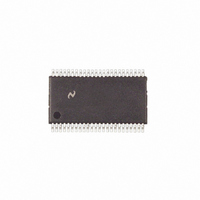
DS90CR562MTD National Semiconductor, DS90CR562MTD Datasheet

DS90CR562MTD
Specifications of DS90CR562MTD
Available stocks
Related parts for DS90CR562MTD
DS90CR562MTD Summary of contents
Page 1
... LVDS devices for low EMI n Low power CMOS design n Power-down mode n PLL requires no external components n Low profile 48-lead TSSOP package n Rising edge data strobe n Compatible with TIA/EIA-644 LVDS standard DS012470-27 Order Number DS90CR562MTD See NS Package Number MTD48 APPLICATION DS012470 July 1997 DS90CR562 DS012470-1 DS012470-2 ...
Page 2
Connection Diagrams DS90CR561 www.national.com DS012470-3 2 DS90CR562 DS012470-4 ...
Page 3
... Absolute Maximum Ratings If Military/Aerospace specified devices are required, please contact the National Semiconductor Sales Office/ Distributors for availability and specifications. Supply Voltage ( CMOS/TTL Input Voltage CMOS/TTL Ouput Voltage LVDS Receiver Input Voltage LVDS Receiver Input Voltage LVDS Output Short Circuit Duration ...
Page 4
Electrical Characteristics Over recommended operating supply and temperature ranges unless otherwise specified Symbol Parameter TRANSMITTER SUPPLY CURRENT I Transmitter Supply Current, CCTZ Power Down RECEIVER SUPPLY CURRENT I Receiver Supply Current, CCRW Worst Case I Receiver Supply Current, CCRG 16 ...
Page 5
Transmitter Switching Characteristics Over recommended operating supply and temperature ranges unless otherwise specified Symbol TPDD Transmitter Powerdown Delay ( Figure 15 ) Note 5: This limit based on bench characterization. Receiver Switching Characteristics Over recommended operating supply and temperature ranges ...
Page 6
AC Timing Diagrams Note 7: The worst case test pattern produces a maximum toggling of device digital circuitry, LVDS I/O and TTL I/O. Note 8: The 16 grayscale test pattern tests device power consumption for a “typical” LCD display pattern. ...
Page 7
AC Timing Diagrams (Continued) Measurements at Vdiff = 0V TCCS measured between earliest and latest initial LVDS edges. TxCLK OUT Differential High Low Edge for DS90CF561 TxCLK OUT Differential Low High Edge for DS90CR561 FIGURE 6. DS90CR561 (Transmitter) Channel-to-Channel Skew ...
Page 8
AC Timing Diagrams FIGURE 10. DS90CR562 (Receiver) Clock In to Clock Out Delay FIGURE 11. DS90CR561 (Transmitter) Phase Lock Loop Set Time FIGURE 12. DS90CR562 (Receiver) Phase Lock Loop Set Time FIGURE 13. Seven Bits of LVDS in One Clock ...
Page 9
AC Timing Diagrams (Continued) FIGURE 14. 21 Parallel TTL Data Inputs Mapped to LVDS Outputs (DS90CR561) FIGURE 15. Transmitter Powerdown Delay FIGURE 16. Receiver Powerdown Delay 9 DS012470-22 DS012470-23 DS012470-24 www.national.com ...
Page 10
AC Timing Diagrams FIGURE 17. Transmitter LVDS Output Pulse Position Measurement SW — Setup and Hold Time (Internal data sampling window) TCCS — Transmitter Output Skew RSKM Cable Skew (type, length) + Source Clock Jitter (cycle to cycle) Cable Skew ...
Page 11
DS90CR561 Pin Description—FPD Link Transmitter Pin Name I/O No Power supply pins for TTL inputs CC GND I 5 Ground pins for TTL inputs PLL Power supply pin for PLL CC PLL GND I ...
Page 12
... NATIONAL’S PRODUCTS ARE NOT AUTHORIZED FOR USE AS CRITICAL COMPONENTS IN LIFE SUPPORT DEVICES OR SYSTEMS WITHOUT THE EXPRESS WRITTEN APPROVAL OF THE PRESIDENT AND GENERAL COUNSEL OF NATIONAL SEMICONDUCTOR CORPORATION. As used herein: 1. Life support devices or systems are devices or systems which, (a) are intended for surgical implant ...


