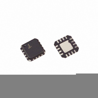
EL1507CL Intersil, EL1507CL Datasheet - Page 14

EL1507CL
Manufacturer Part Number
EL1507CL
Description
IC LINE DRIVER ADSL 16-QFN
Manufacturer
Intersil
Type
Driverr
Datasheet
1.EL1507CL.pdf
(16 pages)
Specifications of EL1507CL
Number Of Drivers/receivers
1/0
Protocol
DSL
Voltage - Supply
12V
Mounting Type
Surface Mount
Package / Case
16-VQFN Exposed Pad, 16-HVQFN, 16-SQFN, 16-DHVQFN
Lead Free Status / RoHS Status
Contains lead / RoHS non-compliant
Available stocks
Company
Part Number
Manufacturer
Quantity
Price
Company:
Part Number:
EL1507CL
Manufacturer:
INTERSIL
Quantity:
354
Part Number:
EL1507CL
Manufacturer:
INTERSIL
Quantity:
20 000
Part Number:
EL1507CLZ
Manufacturer:
INTERSIL
Quantity:
20 000
The overall power dissipation (P
P
Then, the θ
done using the equation:
where:
This θ
needed on the board to dissipate the power.
The SO power packages are designed so that heat may be
conducted away from the device in an efficient manner. To
disperse this heat, the center leads are internally connected
to the mounting platform of the die. Heat flows through the
leads into the circuit board copper, then spreads and
convects to air. Thus, the ground plane on the component
side of the board becomes the heatsink. This has proven to
be a very effective technique. A separate application note
details the 16 Ld QFN PCB design considerations.
Single Supply Operation
The EL1507 can also be powered from a single supply
voltage. When operating in this mode, the GND pins can still
be connected directly to GND. To calculate power
dissipation, the equations in the previous section should be
used, with V
Output Loading
While the drive amplifiers can output in excess of 400mA
transiently, the internal metallization is not designed to carry
more than 75mA of steady DC current and there is no
current-limit mechanism. This allows safely driving rms
sinusoidal currents of 2 x 75mA, or 150mA. This current is
more than that required to drive line impedances to large
output levels, but output short circuits cannot be tolerated.
The series output resistor will usually limit currents to safe
values in the event of line shorts. Driving lines with no series
resistor is a serious hazard.
The amplifiers are sensitive to capacitive loading. More than
25pF will cause peaking of the frequency response. The same
Intersil products are sold by description only. Intersil Corporation reserves the right to make changes in circuit design, software and/or specifications at any time without
notice. Accordingly, the reader is cautioned to verify that data sheets are current before placing orders. Information furnished by Intersil is believed to be accurate and
reliable. However, no responsibility is assumed by Intersil or its subsidiaries for its use; nor for any infringements of patents or other rights of third parties which may result
from its use. No license is granted by implication or otherwise under any patent or patent rights of Intersil or its subsidiaries.
Dquiescent
T
T
P
θ
package when mounted on the PCB
AMB
JA
JUNCT
DISS
JA
is the junction to ambient thermal resistance for the
is the maximum ambient temperature
value is then used to calculate the area of copper
is the dissipation calculated above
is the maximum die temperature (150°C)
JA
and P
S
equal to half the supply rail.
requirement needs to be calculated. This is
All Intersil U.S. products are manufactured, assembled and tested utilizing ISO9000 quality systems.
Dtransistor
θ
JA
Intersil Corporation’s quality certifications can be viewed at www.intersil.com/design/quality
=
For information regarding Intersil Corporation and its products, see www.intersil.com
(
------------------------------------------------ -
T
JUNCT
.
14
P
DISS
DISS
–
T
AMB
) is obtained by adding
)
EL1507
is true of badly terminated lines connected without a series
matching resistor.
Power Supplies
The power supplies should be well bypassed close to the
EL1507. A 3.3µF tantalum capacitor for each supply works well.
Since the load currents are differential, they should not travel
through the board copper and set up ground loops that can
return to amplifier inputs. Due to the class AB output stage
design, these currents have heavy harmonic content. If the
ground terminal of the positive and negative bypass capacitors
are connected to each other directly and then returned to circuit
ground, no such ground loops will occur. This scheme is
employed in the layout of the EL1507 demonstration board,
and documentation can be obtained from the factory.
Feedback Resistor Value
The bandwidth and peaking of the amplifiers varies with supply
voltage somewhat and with gain settings. The feedback resistor
values can be adjusted to produce an optimal frequency
response. Here is a series of resistor values that produce an
optimal driver frequency response (<1dB peaking) for different
supply voltages and gains:
Power Control Function
The EL1507 contains two forms of power control operation.
Two digital inputs, C
current of the EL1507 drive amplifiers. As the supply current is
reduced, the EL1507 will start to exhibit slightly higher levels of
distortion and the frequency response will be limited. The 4
power modes of the EL1507 are set up as shown in the table
below:
TABLE 1. OPTIMUM DRIVER FEEDBACK RESISTOR FOR
C
Voltage
Supply
0
0
1
1
1
±12V
±5V
TABLE 2. POWER MODES OF THE EL1507
VARIOUS GAINS AND SUPPLY VOLTAGES
C
0
1
0
1
0
0
I
¾-I
½-I
Power Down
and C
S
2.5
2k
2k
Full Power Mode
S
S
Power Mode
Power Mode
1
, can be used to control the supply
Driver Voltage Gain
Operation
1.8k
1.8k
5
March 26, 2007
1.5k
1.5k
10
FN7013.3


