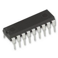
TDA1517P/N3 NXP Semiconductors, TDA1517P/N3 Datasheet - Page 7

TDA1517P/N3
Manufacturer Part Number
TDA1517P/N3
Description
AMP, AUDIO, PWR, 6W, STER, 18HDIP
Manufacturer
NXP Semiconductors
Datasheet
1.TDA1517N3112.pdf
(15 pages)
Specifications of TDA1517P/N3
Amplifier Class
B
No. Of Channels
2
Output Power
12W
Supply Voltage Range
6V To 18V
Thd + N
0.1% @ 1W, 4ohm, VP=14.4V
Load Impedance
4ohm
Operating Temperature Range
-40°C To +85°C
Rohs Compliant
Yes
Available stocks
Company
Part Number
Manufacturer
Quantity
Price
Company:
Part Number:
TDA1517P/N3
Manufacturer:
NXP Semiconductors
Quantity:
1 966
Company:
Part Number:
TDA1517P/N3
Manufacturer:
NXP
Quantity:
20 000
NXP Semiconductors
AC CHARACTERISTICS
V
Notes
1. Output power is measured directly at the output pins of the IC.
2. Frequency response externally fixed.
3. Ripple rejection measured at the output with a source impedance of 0 Ω, maximum ripple amplitude of 2 V (p-p) and
4. Noise voltage measured in a bandwidth of 20 Hz to 20 kHz.
5. Noise output voltage independent of R
2004 Feb 18
P
THD
f
f
G
SVRR
|Z
V
α
|ΔG
P
lr
hr
cs
o
no
2 x 6 W stereo power amplifier
v
i
|
= 14.4 V; R
a frequency between 100 Hz and 10 kHz.
SYMBOL
v
|
L
= 4 Ω; f = 1 kHz; T
output power
total harmonic distortion
low frequency roll-off
high frequency roll-off
closed loop voltage gain
supply voltage ripple rejection
input impedance
noise output voltage
channel separation
channel unbalance
on
mute
standby
on
on
mute
PARAMETER
amb
= 25 °C; measured in Fig.6; unless otherwise specified.
s
(V
I
= 0 V).
THD = 0.5%; note 1
THD = 10%; note 1
P
at −3 dB; note 2
at −1 dB
note 3
R
R
note 5
R
o
s
s
s
= 1 W
= 0 Ω; note 4
= 10 Ω; note 4
= 10 Ω
CONDITIONS
7
4
5.5
−
−
20
19
48
48
80
50
−
−
−
40
−
MIN.
TDA1517; TDA1517P
5
6.0
0.1
45
−
20
−
−
−
60
50
70
50
−
0.1
TYP.
Product specification
−
−
−
−
−
21
−
−
−
75
−
100
−
−
1
MAX.
W
W
%
Hz
kHz
dB
dB
dB
dB
kΩ
μV
μV
μV
dB
dB
UNIT


