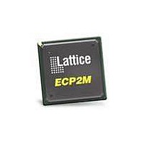
LFE2-12SE-5TN144C Lattice, LFE2-12SE-5TN144C Datasheet - Page 25

LFE2-12SE-5TN144C
Manufacturer Part Number
LFE2-12SE-5TN144C
Description
FPGA - Field Programmable Gate Array 12K LUTs S-Series 1.1.2V -5 Spd
Manufacturer
Lattice
Datasheet
1.LFE2-12E-5FN256C.pdf
(385 pages)
Specifications of LFE2-12SE-5TN144C
Number Of Macrocells
12000
Maximum Operating Frequency
320 MHz
Number Of Programmable I/os
93
Data Ram Size
226304
Delay Time
12 ns
Supply Voltage (max)
1.26 V
Maximum Operating Temperature
+ 85 C
Minimum Operating Temperature
0 C
Package / Case
TQFP-144
Mounting Style
SMD/SMT
Supply Voltage (min)
1.14 V
Lead Free Status / Rohs Status
Details
Available stocks
Company
Part Number
Manufacturer
Quantity
Price
Company:
Part Number:
LFE2-12SE-5TN144C
Manufacturer:
Lattice Semiconductor Corporation
Quantity:
10 000
- Current page: 25 of 385
- Download datasheet (3Mb)
Lattice Semiconductor
Table 2-7. Maximum Number of Elements in a Block
Some options are available in four elements. The input register in all the elements can be directly loaded or can be
loaded as a shift register from previous operand registers. By selecting “dynamic operation” the following opera-
tions are possible:
• In the ‘Signed/Unsigned’ options the operands can be switched between signed and unsigned on every cycle.
• In the ‘Add/Sub’ option the Accumulator can be switched between addition and subtraction on every cycle.
• The loading of operands can switch between parallel and serial operations.
MULT sysDSP Element
This multiplier element implements a multiply with no addition or accumulator nodes. The two operands, A and B,
are multiplied and the result is available at the output. The user can enable the input/output and pipeline registers.
Figure 2-23 shows the MULT sysDSP element.
Figure 2-23. MULT sysDSP Element
MULT
MAC
MULTADDSUB
MULTADDSUBSUM
Width of Multiply
Multiplicand
Multiplier
Signed A
Signed B
Shift Register B Out
Shift Register B In
n
Register B
Input Data
n
n
n
Register
Register
Input
Input
x9
8
2
4
2
m
Register A
Input Data
m
m
Shift Register A Out
m
Shift Register A In
2-22
Multiplier
Multiplier
m
n
To
To
Multiplier
Register
Pipeline
x
CLK (CLK0,CLK1,CLK2,CLK3)
CE (CE0,CE1,CE2,CE3)
RST(RST0,RST1,RST2,RST3)
x18
4
2
2
1
LatticeECP2/M Family Data Sheet
(default)
m+n
m+n
Output
Architecture
x36
—
—
—
1
Related parts for LFE2-12SE-5TN144C
Image
Part Number
Description
Manufacturer
Datasheet
Request
R

Part Number:
Description:
FPGA - Field Programmable Gate Array 12K LUTs S-Series 1.1.2V -6 Spd
Manufacturer:
Lattice
Datasheet:
Part Number:
Description:
FPGA LatticeECP2 Family 12000 Cells 90nm (CMOS) Technology 1.2V 256-Pin FBGA
Manufacturer:
LATTICE SEMICONDUCTOR
Datasheet:

Part Number:
Description:
IC FPGA 12KLUTS 193I/O 256-BGA
Manufacturer:
Lattice
Datasheet:

Part Number:
Description:
IC FPGA 12KLUTS 93I/O 144-TQFP
Manufacturer:
Lattice
Datasheet:

Part Number:
Description:
IC FPGA 12KLUTS 131I/O 208-BGA
Manufacturer:
Lattice
Datasheet:

Part Number:
Description:
IC FPGA 12KLUTS 297I/O 484-BGA
Manufacturer:
Lattice
Datasheet:

Part Number:
Description:
IC FPGA 12KLUTS 297I/O 484-BGA
Manufacturer:
Lattice
Datasheet:

Part Number:
Description:
IC FPGA 12KLUTS 144TQFP
Manufacturer:
Lattice
Datasheet:

Part Number:
Description:
IC FPGA 12KLUTS 208PQFP
Manufacturer:
Lattice
Datasheet:

Part Number:
Description:
IC FPGA 12KLUTS 144TQFP
Manufacturer:
Lattice
Datasheet:

Part Number:
Description:
IC FPGA 12KLUTS 208PQFP
Manufacturer:
Lattice
Datasheet:

Part Number:
Description:
IC FPGA 12KLUTS 256FPBGA
Manufacturer:
Lattice
Datasheet:


