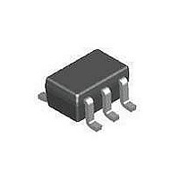
SIP32411DR-T1-GE3 Vishay, SIP32411DR-T1-GE3 Datasheet

SIP32411DR-T1-GE3
Specifications of SIP32411DR-T1-GE3
Available stocks
Related parts for SIP32411DR-T1-GE3
SIP32411DR-T1-GE3 Summary of contents
Page 1
... Document Number: 66710 S11-0367-Rev. D, 07-Mar-11 FEATURES • 1 5.5 V operation voltage range • 62 mΩ typical from for SiP32411DN • 101 mΩ typical from for SiP32411DR • Low R ON • Slew rate controlled turn-on: 150 µs at 3.6 V • Fast shutdown load discharge • ...
Page 2
... MBxx TDFN4 1 1.6 mm AEx SC70-6 package ) TDFN4 1 1.6 mm SC70-6 package TDFN4 1 1 pin SC70 pin TDFN4 1 1 pin SC70 pin TDFN4 1 1.6 mm Limit 1 Part Number SiP32411DR-T1-GE3 SiP32411DNP-T1-GE4 Limit Unit - 0.3 IN 1.8 2.4 A 2.2 3 4000 125 °C 240 °C/W ...
Page 3
... RDS TDFN4 1 1.6 mm package inactive ° Ω 3 LOAD SiP32411 Vishay Siliconix Limits - 40 ° ° Min. Typ. Max. 1.1 - 5 °C - 105 125 A 120 = 25 °C - 101 °C - 101 120 °C - 101 120 °C - 101 120 ° ...
Page 4
... SiP32411 Vishay Siliconix PIN CONFIGURATION OUT 1 2 GND EN 3 Top View Figure 2 - SC70-6 Package PIN DESCRIPTION Pin Number Name SC70-6 TDFN4 This pin is the n-channel MOSFET drain connection. Bypass to ground through a 2.2 µF capacitor GND Ground connection Enable input 1 1 OUT This pin is the n-channel MOSFET source connection. Bypass to ground through a 0.1 µ ...
Page 5
... DS(on) IN Document Number: 66710 S11-0367-Rev. D, 07-Mar-11 1000 0.01 0.001 4.0 4.5 5 4.0 4.5 5.0 5.5 for TDFN4 package 4.0 4.5 5.0 5.5 SiP32411 Vishay Siliconix 100 Temperature (°C) Figure 9 - Off Switch Current vs. Temperature 85 TDFN4 1 1.6 mm package 0.1 A ...
Page 6
... SiP32411 Vishay Siliconix TYPICAL CHARACTERISTICS (internally regulated, 25 °C, unless otherwise noted) 600 550 500 450 400 350 300 250 200 150 100 1.0 1.5 2.0 2.5 3.0 3.5 V (V) IN Figure 14 - Output Pull Down vs. Input Voltage 100 0.1 0.01 1.0 1.5 2 ...
Page 7
... TYPICAL CHARACTERISTICS (internally regulated, 25 °C, unless otherwise noted) TYPICAL WAVEFORMS Figure 21 - Switching (V IN Figure 23 - Switching (V Document Number: 66710 S11-0367-Rev. D, 07-Mar-11 0. 0.1 µ Ω 0.18 0.16 0.14 0.12 0. Temperature (°C) Figure 20 - Turn-Off Delay Time vs. Temperature = 3 SiP32411 Vishay Siliconix 60 80 100 Figure 22 - Turn-Off ( Figure 24 - Turn-Off ( www.vishay.com 7 ...
Page 8
... SiP32411 Vishay Siliconix BLOCK DIAGRAM IN EN PCB LAYOUT Top Figure 26 - PCB Layout for TDFN4 1 1.6 mm (board size: 1 inch x 1 inch) Top Figure 27 - PCB Layout for SC70-6 (board size: 1 inch x 1 inch) www.vishay.com 8 Reverse Blocking Charge Control Turn-On Pump Logic Slew Rate ...
Page 9
... Vishay Siliconix maintains worldwide manufacturing capability. Products may be manufactured at one of several qualified locations. Reliability data for Silicon Technology and Package Reliability represent a composite of all qualified locations. For related documents such as package/tape drawings, part marking, and reliability data, see www ...
Page 10
... NOM. MAX. 0.55 0.60 - 0.05 0.15 REF 0.25 0.30 1.20 1.25 0.86 0.91 0.50 BSC 1.60 1.65 0.50 0. 0.35 0.40 Package Information Vishay Siliconix D2 b Pin # (Optional Bottom View INCHES MIN. NOM. MAX. 0.020 0.022 0.024 0.00 - 0.002 0.006 0.008 0.010 ...
Page 11
... Dimension “D” and “E1” are determined at the outer most extremes of the plastic body exclusive of mold flash, tie bar burrs, gate burrs and interlead flash, but including any mismatch between the top and bottom of the plastic body. Package Information Vishay Siliconix A A See Detail A U1 ...
Page 12
... Package Information Vishay Siliconix Dim ECN: S-42145—Rev. A, 22-Nov-04 DWG: 5941 www.vishay.com 2 MILLIMETERS Min Nom Max Min 0.80 − 1.10 0.031 0.00 − 0.10 0.000 0.80 0.90 1.00 0.031 0.15 − 0.30 0.006 0.15 0.20 0.25 0.006 0.08 − 0.25 0.003 ...
Page 13
... Vishay product could result in personal injury or death. Customers using or selling Vishay products not expressly indicated for use in such applications their own risk and agree to fully indemnify and hold Vishay and its distributors harmless from and against any and all claims, liabilities, expenses and damages arising or resulting in connection with such use or sale, including attorneys fees, even if such claim alleges that Vishay or its distributor was negligent regarding the design or manufacture of the part ...


