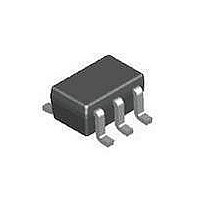
SIP32411DR-T1-GE3 Vishay, SIP32411DR-T1-GE3 Datasheet - Page 2

SIP32411DR-T1-GE3
Manufacturer Part Number
SIP32411DR-T1-GE3
Description
Power Switch ICs - Power Distribution 2A 1.2V Slew Rate Ctrl Load Switch
Manufacturer
Vishay
Series
-r
Type
High Sider
Datasheet
1.SIP32411DR-T1-GE3.pdf
(13 pages)
Specifications of SIP32411DR-T1-GE3
On Resistance (max)
76 mOhms
Maximum Operating Temperature
+ 85 C
Minimum Operating Temperature
- 40 C
Package / Case
SC70-6
Maximum Power Dissipation
324 mW
Mounting Style
SMD/SMT
Number Of Switches
Single
Off Time (max)
1 us
On Time (max)
210 us
Supply Current
2 A
Supply Voltage (max)
5.5 V
Supply Voltage (min)
1.1 V
Switch Configuration
Single
Switch Current (typ)
2.4 A
Input Type
Non-Inverting
Number Of Outputs
1
On-state Resistance
101 mOhm
Current - Output / Channel
2A
Current - Peak Output
2.2A
Voltage - Supply
1.1 V ~ 5.5 V
Operating Temperature
-40°C ~ 85°C
Mounting Type
Surface Mount
Lead Free Status / Rohs Status
Details
Available stocks
Company
Part Number
Manufacturer
Quantity
Price
Company:
Part Number:
SIP32411DR-T1-GE3
Manufacturer:
TI
Quantity:
101
Part Number:
SIP32411DR-T1-GE3
Manufacturer:
VISHAY/威世
Quantity:
20 000
SiP32411
Vishay Siliconix
Notes:
x = Lot Code
GE3 and GE4 denote halogen-free and RoHS compliant
Notes:
a. Device mounted with all leads and power pad soldered or welded to PC board, see PCB layout.
b. Derate 4.5 mW/°C above T
c. Derate 5.9 mW/°C above T
Stresses beyond those listed under "Absolute Maximum Ratings" may cause permanent damage to the device. These are stress ratings only, and functional operation
of the device at these or any other conditions beyond those indicated in the operational sections of the specifications is not implied. Exposure to absolute maximum
rating/conditions for extended periods may affect device reliability.
www.vishay.com
2
ORDERING INFORMATION
ABSOLUTE MAXIMUM RATINGS
Parameter
Supply Input Voltage (V
Enable Input Voltage (V
Output Voltage (V
Maximum Continuous Switch Current (I
Maximum Pulsed Current (I
(Pulsed at 1 ms, 10 % Duty Cycle)
ESD Rating (HBM)
Junction Temperature (T
Thermal Resistance (θ
Power Dissipation (P
RECOMMENDED OPERATING RANGE
Parameter
Input Voltage Range (V
Operating Temperature Range
Temperature Range
- 40 °C to 85 °C
OUT
D
)
)
JA
a
IN
IN
EN
J
)
)
)
)
a
)
DM
A
A
= 70 °C, see PCB layout.
= 70 °C, see PCB layout.
) V
IN
MAX
)
TDFN4 1.2 mm x 1.6 mm
SC70-6 package
TDFN4 1.2 mm x 1.6 mm
SC70-6 package
TDFN4 1.2 mm x 1.6 mm
6 pin SC70-6
4 pin TDFN4 1.2 mm x 1.6 mm
6 pin SC70-6
4 pin TDFN4 1.2 mm x 1.6 mm
Package
SC70-6
b
b
c
c
Marking
1.1 to 5.5
- 40 to 85
MBxx
AEx
Limit
- 0.3 to V
- 40 to 125
- 0.3 to 6
- 0.3 to 6
Limit
4000
240
170
230
324
1.8
2.4
2.2
3
IN
SiP32411DNP-T1-GE4
SiP32411DR-T1-GE3
+ 0.3
Part Number
S11-0367-Rev. D, 07-Mar-11
Document Number: 66710
Unit
°C
V
°C/W
Unit
mW
°C
V
A
V


