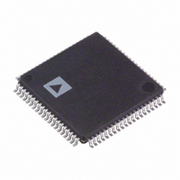
ADV7194KSTZ Analog Devices Inc, ADV7194KSTZ Datasheet - Page 17

ADV7194KSTZ
Manufacturer Part Number
ADV7194KSTZ
Description
IC ENCODER VIDEO EXT-10 80-LQFP
Manufacturer
Analog Devices Inc
Type
Video Encoderr
Datasheet
1.ADV7194KSTZ.pdf
(69 pages)
Specifications of ADV7194KSTZ
Applications
DVD, PC Video, Multimedia
Voltage - Supply, Analog
3.3 V ~ 5 V
Voltage - Supply, Digital
3.3 V ~ 5 V
Mounting Type
Surface Mount
Package / Case
80-LQFP
Input Format
Digital
Output Format
Analog
Supply Voltage Range
3.15V To 3.6V
Operating Temperature Range
0°C To +70°C
Tv / Video Case Style
LQFP
No. Of Pins
80
Msl
MSL 1 - Unlimited
Svhc
No SVHC
Rohs Compliant
Yes
Lead Free Status / RoHS Status
Lead free / RoHS Compliant
For Use With
EVAL-ADV7194EB - BOARD EVAL FOR ADV7194
Lead Free Status / RoHS Status
Lead free / RoHS Compliant, Lead free / RoHS Compliant
Available stocks
Company
Part Number
Manufacturer
Quantity
Price
Company:
Part Number:
ADV7194KSTZ
Manufacturer:
ADI
Quantity:
393
Company:
Part Number:
ADV7194KSTZ
Manufacturer:
ADI
Quantity:
717
Company:
Part Number:
ADV7194KSTZ
Manufacturer:
Analog Devices Inc
Quantity:
10 000
Part Number:
ADV7194KSTZ
Manufacturer:
ADI/亚德诺
Quantity:
20 000
FEATURES—FUNCTIONAL DESCRIPTION
BLACK BURST OUTPUT
It is possible to output a black burst signal from two DACs. This
signal output is very useful for professional video equipment
since it enables two video sources to be locked together. (Mode
Register 9.)
BRIGHTNESS DETECT
This feature is used to monitor the average brightness of the
incoming Y video signal on a field by field basis. The informa-
tion is read from the I
saturation, contrast and brightness controls can be adjusted
(for example to compensate for very dark pictures). (Bright-
ness Detect Register.)
CHROMA/LUMA DELAY
The luminance data can be delayed by maximum of six clock
cycles. Additionally the Chroma can be delayed by a maximum
of eight clock cycles (one clock cycle at 27 MHz). (Timing Reg-
ister 0 and Mode Register 9.)
CLAMP OUTPUT
The ADV7194 has a programmable clamp TTL output signal.
This clamp signal is programmable to the front and back porch.
The clamp signal can be varied by one to three clock cycles in
a positive and negative direction from the default position. (Mode
Register 5, Mode Register 7.)
MR57 = 0
CLAMP O/P SIGNALS
MR57 = 1
DIGITAL DATA
DIGITAL DATA
GENERATOR
GENERATOR
CHROMA DELAY
BLACK BURST OUTPUT
2
C and based on this information the color
ADV7194
ADV7194
CVBS
CVBS
LUMA DELAY
CVBS
OUTPUT PIN
CLAMP
OUTPUT PIN
CSO, HSO, AND VSO OUTPUTS
The ADV7194 supports three output timing signals, CSO (com-
posite sync signal), HSO (Horizontal Sync Signal) and VSO
(Vertical Sync Signal). These output TTL signals are aligned
with the analog video outputs. See Figure 31 for an example
of these waveforms. (Mode Register 7.)
COLOR BAR GENERATION
The ADV7194 can be configured to generate 100/7.5/75/7.5
color bars for NTSC or 100/0/75/0 color bars for PAL. (Mode
Register 4.)
COLOR BURST SIGNAL CONTROL
The burst information can be switched on and off the composite
and chroma video output. (Mode Register 4.)
COLOR CONTROLS
The ADV7194 allows the user to control the brightness, contrast,
hue and saturation of the color. The control registers may be
double-buffered, meaning that any modification to the registers
will be done outside the active video region and, therefore, changes
made will not be visible during active video.
Contrast Control
Contrast adjustment is achieved by scaling the Y input data by a
factor programmed by the user. This factor allows the data to be
scaled between 0% and 150%. (Contrast Control Register.)
Brightness Control
The brightness is controlled by adding a programmable setup level
onto the scaled Y data. This brightness level may be added onto
the Y data. For NTSC with pedestal, the setup can vary from
0 IRE to 22.5 IRE. For NTSC without pedestal and PAL, the
setup can vary from –7.5 IRE to +15 IRE. (Brightness Control
Register.)
Color Saturation
Color adjustment is achieved by scaling the Cr and Cb input
data by a factor programmed by the user. This factor allows the
data to be scaled between 0% and 200%. (U Scale Register and
V Scale Register.)
Hue Adjust Control
The hue adjustment is achieved on the composite and chroma
outputs by adding a phase offset onto the color subcarrier in the
active video but leaving the color burst unmodified, i.e., only
the phase between the video and the colorburst is modified and
hence the hue is shifted. The ADV7194 provides a range of
± 22° in increments of 0.17578125°. (Hue Adjust Register.)
CHROMINANCE CONTROL
The color information can be switched on and off the com-
posite, chroma and color component video outputs. (Mode
Register 4.)
EXAMPLE:- NTSC
OUTPUT
VIDEO
CSO
HSO
VSO
525
1
2
CSO HSO VSO
3
4
5
6
7
ADV7194
8
9
10
11–19


