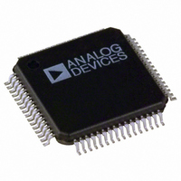
ADV7311KST Analog Devices Inc, ADV7311KST Datasheet - Page 38

ADV7311KST
Manufacturer Part Number
ADV7311KST
Description
IC VID ENC 6-12BIT DAC'S 64LQFP
Manufacturer
Analog Devices Inc
Type
Video Encoderr
Datasheet
1.ADV7311KST.pdf
(84 pages)
Specifications of ADV7311KST
Rohs Status
RoHS non-compliant
Applications
DVD, SD/HD
Voltage - Supply, Analog
2.5V
Voltage - Supply, Digital
2.5V
Mounting Type
Surface Mount
Package / Case
64-LQFP
Input Format
Digital
Output Format
Analog
Supply Voltage Range
2.375V To 2.625V
Operating Temperature Range
0°C To +70°C
Tv / Video Case Style
LQFP
No. Of Pins
64
Msl
MSL 1 - Unlimited
Lead Free Status / RoHS Status
Lead free / RoHS Compliant
Available stocks
Company
Part Number
Manufacturer
Quantity
Price
Company:
Part Number:
ADV7311KST
Manufacturer:
ADI
Quantity:
300
Company:
Part Number:
ADV7311KST
Manufacturer:
Analog Devices Inc
Quantity:
10 000
Part Number:
ADV7311KSTZ
Manufacturer:
ADI/亚德诺
Quantity:
20 000
ADV7310/ADV7311
Vertical Blanking Interval
The ADV7310/ADV7311 accept input data that contains VBI
data [CGMS, WSS, VITS, and so on] in SD and HD modes.
For SMPTE 293M [525p] standards, VBI data can be inserted
on Lines 13 to 42 of each frame, or on Lines 6 to 43 for the
ITU-R BT.1358 [625p] standard.
For SD NTSC this data can be present on Lines 10 to 20, and
in PAL on Lines 7 to 22.
If VBI is disabled [Address 11h, Bit 4 for HD; Address 43h,
Bit 4 for SD], VBI data is not present at the output and the
entire VBI is blanked. These control bits are valid in all master
and slave modes.
In Slave Mode 0, if VBI is enabled, the blanking bit in the
EAV/SAV code is overwritten, and it is possible to use VBI in
this timing mode as well.
In Slave Mode 1 or 2, the BLANK control bit must be set to
enabled [Address 4Ah, Bit 3] to allow VBI data to pass through
the ADV7310/ADV7311. Otherwise, the ADV7310/ADV7311
automatically blanks the VBI to standard.
If CGMS is enabled and VBI is disabled, the CGMS data will
nevertheless be available at the output.
NTSC/PAL M SYSTEM
(525 LINES/60Hz)
(625 LINES/50Hz)
HSYNC
BLANK
PIXEL
FIELD
DATA
INPUT PIXELS
PAL SYSTEM
ANALOG
VIDEO
NTSC = 44 CLOCK CYCLES
PAL = 44 CLOCK CYCLES
Y
END OF ACTIVE
VIDEO LINE
C
r
Y
F
F
4 CLOCK
4 CLOCK
EAV CODE
0
0
Figure 34. EAV/SAV Embedded Timing
0
0
X
Y
Figure 35. Active Pixel Timing
8
0
1
0
8
0
1
0
ANCILLARY DATA
–38–
0
0
272 CLOCK
344 CLOCK
F
F
(HANC)
F
F
Subcarrier Frequency Registers
[Subaddress 4Ch–4Fh]
Four 8-bit registers are used to set up the subcarrier frequency.
The value of these registers is calculated using the equation
*Rounded to the nearest integer
For example, in NTSC mode,
Subcarrier Register Value = 21F07C1Eh
SD F
SD F
SD F
SD F
Refer to the MPU Port Description section for more details on
how to access the subcarrier frequency registers.
Square Pixel Timing
[Register 42h, Bit 4]
In square pixel mode, the following timing diagrams apply.
Subcarrier Frequency Register
Number of subcarrier frequency values in one video line
A
B
Subcarrier FrequencyValue =
A
B
Number of 27 MHz clk cycles in one video line
A
B
SC
SC
SC
SC
Register 0: 1Eh
Register 1: 7Ch
Register 2: F0h
Register 3: 21h
8
0
1
0
8
0
1
0
SAV CODE
4 CLOCK
F
F
4 CLOCK
START OF ACTIVE
0
0
NTSC = 208 CLOCK CYCLES
PAL = 136 CLOCK CYCLES
VIDEO LINE
0
0
X
Y
C
b
Cb
Y C
1280 CLOCK
1536 CLOCK
=
r
Y
Y
227.5
1716
C
b
Y
Cr
C
r
×
Y
Y
C
b
2
23
=
569408542
REV. A
2
23
*


