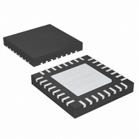
MAX9526ATJ+ Maxim Integrated Products, MAX9526ATJ+ Datasheet - Page 12

MAX9526ATJ+
Manufacturer Part Number
MAX9526ATJ+
Description
IC VID DECODER NTSC/PAL 32-TQFN
Manufacturer
Maxim Integrated Products
Type
Video Decoderr
Datasheet
1.MAX9526AEI.pdf
(38 pages)
Specifications of MAX9526ATJ+
Applications
Automotive Systems, Players, TV
Voltage - Supply, Analog
1.8V
Voltage - Supply, Digital
1.8V
Mounting Type
Surface Mount
Package / Case
32-TQFN Exposed Pad
Lead Free Status / RoHS Status
Lead free / RoHS Compliant
Low-Power, High-Performance
NTSC/PAL Video Decoder
The sync processing block extracts the sync information
and automatically detects 525 line or 625 line inputs.
The PLL operates in either line-locked clock (LLC)
mode or async mode. Selection of the mode is con-
trolled automatically by the MAX9526 or can optionally
be overwritten with the LLC_MODE bits in PLL Control
register 0x0E.
In LLC mode, a hybrid analog/digital PLL generates a
low-jitter line-locked clock. The 54MHz sample clock is
synchronous to the input video. The LLC clock output is
also synchronous to the input video. The ITU output has
the correct number of samples per line and lines per
field. The PLL is designed to lock to signals with up to
160ns peak jitter. When the jitter exceeds the 160ns
peak, the PLL coasts until the jitter improves. If the jitter
continuously exceeds the 160ns peak, the PLL relocks
and the HLOCK status bit in register 0x00 is set to 0.
In LLC mode, the bandwidth of the PLL can be option-
ally programmed to one of eight values between 180Hz
and 2000Hz using the PLLBW bits in PLL Control regis-
ter 0x0E. The default value for the PLL bandwidth is
500Hz.
In async mode, the sample clock frequency is generat-
ed by multiplying the crystal frequency by a factor of
two and the video signal is sampled asynchronously
with the 2x crystal clock. To eliminate artifacts, the
MAX9526 uses an adaptive poly-phase filter to correct
timing and phase errors introduced by the asynchro-
nous sampling. The LLC output is generated by divid-
ing the 54MHz sampling clock by two.
The ITU output in async mode has the correct number of
lines per frame and the correct number of pixels per line
except on the first line of each field. The timing correc-
tion block uses this line to compensate for timing errors
between the incoming video signal and the crystal. As a
result, the first line of each field is longer or shorter for
several pixels depending on the magnitude of the fre-
quency difference between the incoming video signal
and the local crystal. For example, a 100ppm frequency
difference between the incoming video signal and the
crystal results in approximately 23 extra or fewer pixels
on the first line of each field. Line length errors on line
one are of no consequence for most applications since it
is in the vertical blanking interval and does not contain
active video or any other type of data.
The types of inputs that cause the PLL to automatically
switch to async mode are video inputs with a nonstan-
dard carrier frequency. For standard video, the carrier
12
______________________________________________________________________________________
Clock Generator and PLL
Sync Processing
frequency is always a precise multiple of the horizontal
frequency. A typical nonstandard input is video cassette
recorders in which the carrier is not a precise multiple of
the horizontal frequency. The nonstandard detect
(NONSTD) status from the decoder is used to automati-
cally switch the PLL to async mode when nonstandard
carrier frequencies are detected. The NONSTD status is
monitored in the Status register 0x00.
In addition to automatic configuration, the MAX9526
can also be manually configured to provide maximum
flexibility in setting the clock inputs and outputs of the
chip. Table 1 summarizes the clocking modes that are
supported.
Figure 3 shows a block diagram of the digital compos-
ite decoder. This block converts the digitized compos-
ite video signal to digital component video.
The sync extraction function extracts the raw sync sig-
nals from the video and the extracted sync information
is sent to the sync processor. The sync level from the
AFE is code 32 (decimal) on a 10-bit scale and the
blanking level is approximately 208 (decimal) codes
above the sync level. The sync slicer default threshold
is set to approximately the middle of the sync pulse at
decimal code 128. The sync slice level can optionally
be manually adjusted using the slice bits in register
0x0F.
The sync level correction block features an optional
digital clamp that can be enabled in register 0x09.
Enabling the digital clamp sets the sync level to code 0
(decimal) and gives higher frequency tracking of the
input signals. When the digital clamp is enabled, the
sync slice level in register 0x0F should be adjusted
accordingly to provide equivalent noise rejection.
The sync processor extracts the horizontal sync and
vertical sync signals. Field pulses and burst gate puls-
es are generated based on VSYNC and HSYNC,
respectively. The sync processing block provides sync
timing to measure the sync level and amplitude for the
black level control and composite AGC. The sync
processor also detects incoming video signal stan-
dards (525 line NTSC and 625 line PAL). Video stan-
dard information is available in Status register 0x01.
The detected video standard is used to automatically
configure the decoder. The MAX9526 detects NTSC-M
(standard NTSC) and PAL B/G/H/I/D (standard PAL)
Sync Level Correction and Sync Extraction
Sync Processor and Analog Copy
Digital Composite Decoding
Protection Detection
Clocking Modes


