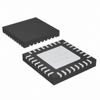
MAX9526ATJ+ Maxim Integrated Products, MAX9526ATJ+ Datasheet - Page 2

MAX9526ATJ+
Manufacturer Part Number
MAX9526ATJ+
Description
IC VID DECODER NTSC/PAL 32-TQFN
Manufacturer
Maxim Integrated Products
Type
Video Decoderr
Datasheet
1.MAX9526AEI.pdf
(38 pages)
Specifications of MAX9526ATJ+
Applications
Automotive Systems, Players, TV
Voltage - Supply, Analog
1.8V
Voltage - Supply, Digital
1.8V
Mounting Type
Surface Mount
Package / Case
32-TQFN Exposed Pad
Lead Free Status / RoHS Status
Lead free / RoHS Compliant
Low-Power, High-Performance
NTSC/PAL Video Decoder
ABSOLUTE MAXIMUM RATINGS
AVDD to AGND .......................................................-0.3V to +2V
DVDD to DGND ........................................................-0.3V to +2V
DVDDIO to DGND .................................................-0.3V to +3.6V
AGND to DGND.....................................................-0.1V to +0.1V
D9–D0, LLC to DGND .........................-0.3V to (DVDDIO + 0.3V)
V
XTAL/OSC, XTAL2 to AGND ....................................-0.3V to +2V
IRQ, SDA, SCL, DEVADR to DGND ......................-0.3V to +3.6V
Continuous Current In/Out All Pins ...................................±50mA
Continuous Power Dissipation (T
ELECTRICAL CHARACTERISTICS
(V
T
Stresses beyond those listed under “Absolute Maximum Ratings” may cause permanent damage to the device. These are stress ratings only, and functional
operation of the device at these or any other conditions beyond those indicated in the operational sections of the specifications is not implied. Exposure to
absolute maximum rating conditions for extended periods may affect device reliability.
2
SUPPLIES
Analog Supply Voltage Range
Digital Supply Voltage Range
Digital I/O Supply Voltage Range
Analog Supply Current
(Note 2)
Digital Supply Current
(Note 2)
Digital I/O Supply Current
(Note 2)
VIDEO INPUTS, V
Input Voltage Range
Input Resistance
Input Capacitance
Video Input Reference Voltage
(V
Sync-Tip Clamp Level
Input Clamping Current
A
IN1
AVDD
28-Pin QSOP Single-Layer Board
= +25°C.) (Note 1)
REF
(derate 10.8mW/°C above +70°C) .............................860mW
, V
_______________________________________________________________________________________
)
IN2
= V
, V
PARAMETER
DVDD
REF
to AGND .......................-0.3V to (AVDD + 0.3V)
= +1.8V, V
REF
, AND CLAMP
DVDDIO
A
= +70°C)
= +3.3V, V
SYMBOL
DVDDIO
I
V
DVDDIO
AVDD
DVDD
I
I
V
CLMP2
AVDD
DVDD
R
C
REF
IN
IN
AGND
Normal operation
Sleep mode
Shutdown
Normal operation
Sleep mode
Shutdown
Normal operation, V
Normal operation, V
Sleep mode, V
Shutdown, V
Guaranteed by full-scale conversion range
Activity detect clamp
Activity detect clamp,
V
VIN
= V
= V
DGND
CLMP2
DVDDIO
= 0V, T
DVDDIO
CONDITIONS
+ 150mV
Operating Temperature Range .........................-40°C to +125°C
Junction Temperature ......................................................+150°C
Storage Temperature Range .............................-65°C to +150°C
Lead Temperature (soldering, 10s) .................................+300°C
Soldering Temperature (reflow) .......................................+260°C
DVDDIO
DVDDIO
A
= 3.3V
= T
28-Pin QSOP Multilayer Board
32-Pin TQFN Multilayer Board
= 3.3V
(derate 12.6mW°C above +70°C) ............................1009mW
(derate 20.8mW/°C above +70°C) ...........................1663mW
MIN
= 1.8V
= 3.3V
to T
MAX
, unless otherwise noted. Typical values are at
MIN
0.27
1.7
1.7
1.7
TYP
850
550
1.8
1.8
3.3
2.2
0.5
3.5
6.4
0.8
0.8
0.5
2.0
42
70
5
5
2
8
MAX
1000
1000
0.83
3.45
100
110
1.9
1.9
55
10
10
3
UNITS
V
MΩ
mA
mA
mA
mV
mV
µA
µA
µA
pF
µA
V
V
V
P-P


