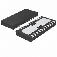
LTC6605CDJC-10#PBF Linear Technology, LTC6605CDJC-10#PBF Datasheet - Page 14

LTC6605CDJC-10#PBF
Manufacturer Part Number
LTC6605CDJC-10#PBF
Description
IC FILTER 10MHZ DUAL 22-DFN
Manufacturer
Linear Technology
Datasheet
1.LTC6605CDJC-10PBF.pdf
(20 pages)
Specifications of LTC6605CDJC-10#PBF
Filter Type
Antialiasing
Frequency - Cutoff Or Center
5MHz
Number Of Filters
2
Max-order
2nd
Voltage - Supply
2.7 V ~ 5.25 V
Mounting Type
Surface Mount
Package / Case
22-DFN
No. Of Amplifiers
2
Input Offset Voltage
1mV
Gain Db Max
14dB
Bandwidth
10MHz
Supply Voltage Range
2.7V To 5.25V
Supply Current
33.1mA
Amplifier Case Style
DFN
No. Of Pins
22
Rohs Compliant
Yes
Lead Free Status / RoHS Status
Lead free / RoHS Compliant
Available stocks
Company
Part Number
Manufacturer
Quantity
Price
LTC6605-10
APPLICATIONS INFORMATION
Input Impedance
Calculating the low frequency input impedance depends
on how the inputs are driven.
Figure 6 shows a simplifi ed low frequency equivalent
circuit. For balanced input sources (V
low frequency input impedance is given by the equation:
Therefore, the differential input impedance is simply:
For single-ended inputs (V
increases over the balanced differential case due to the
fact that the summing node (at the junction of R1, R2
and R3) moves in phase with V
impedance. Referring to Figure 6 with V
impedance looking into either input is:
Input Common Mode Voltage Range
The input common mode voltage is defi ned as the average
of the two inputs into resistor R1:
The input common mode range is a function of the fi lter
confi guration (GAIN), V
Referring to Figure 6, the summing junction where R1, R2
and R3 merge together should not swing within 1.4V of
the V
14
R
R
R
V
INP
IN(DIFF)
INCM
INP
+
power supply. Additionally, to avoid forward biasing
V
V
INM
INP
= R
= R
=
+
–
–
+
INM
= 2 • R1
INM
V
R
R
INM
INP
INP
= R1
Figure 6. Input Impedance
+
R1
R1
2
1
V
INM
2
1
INDIFF
R3
R3
•
INM
R1
R1+ R2
R2
R2
+
–
R2
= 0), the input impedance
INP
and the V
to bootstrap the input
INP
INM
660510 F06
0.1μF
OCM
= –V
–
+
= 0, the input
V
V
V
V
OUTDIFF
OUT
OUT
OCM
potential.
INM
–
+
), the
the ESD protection diodes on the input pins, neither input
should swing further than 325mV below the V
rail. Therefore, the input common mode voltage should
be constrained to:
The specifi cations in the Electrical Characteristics table are
a special case of the general equation above. For a single
3V power supply, (V
ΔV
mode range is:
Likewise, for a single 5V power supply, (V
with V
valid input common mode range is:
Output Common Mode and V
The output common mode voltage is defi ned as the aver-
age of the two outputs:
As the equation shows, the output common mode voltage
is independent of the input common mode voltage, and
is instead determined by the voltage on the V
means of an internal feedback loop.
If the V
develops a potential halfway between the V
ages. The V
if desired. For example, when driving an ADC, if the ADC
makes a reference available for setting the common mode
voltage, it can be directly tied to the V
ADC is capable of driving the input impedance presented by
the V
(R
the valid range that can be applied to the V
VOCM
–200mV ≤ V
–200mV ≤ V
V
• V
INDIFF
V
OUTCM
(
OCM
OCM
+
). The Electrical Characteristics table also specifi es
OCM
325mV +
= ±0.25V and R1 = R2, the valid input common
pin as listed in the Electrical Characteristics table
1.4V
= 2.5V, ΔV
OCM
=
pin is left open, an internal resistor divider
V
INCM
INCM
OCM
pin can be overdriven to another voltage
)
V
≤ 1.7V
≤ 4.7V
INDIFF
+
R2
=
R1
2
= 3V, V
INDIFF
V
OUT
V
OCM
+
= ±0.25V and R1 = R2, the
V
OCM
–
+
2
INCM
= 0V) with V
V
OUT
Pin
OCM
−
1+
pin, as long as the
+
= 5V, V
OCM
R2
R1
+
and V
OCM
OCM
pin.
–
= 1.5V,
pin, by
–
power
–
= 0V)
660510f
volt-


