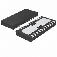
LTC6605CDJC-10#PBF Linear Technology, LTC6605CDJC-10#PBF Datasheet - Page 16

LTC6605CDJC-10#PBF
Manufacturer Part Number
LTC6605CDJC-10#PBF
Description
IC FILTER 10MHZ DUAL 22-DFN
Manufacturer
Linear Technology
Datasheet
1.LTC6605CDJC-10PBF.pdf
(20 pages)
Specifications of LTC6605CDJC-10#PBF
Filter Type
Antialiasing
Frequency - Cutoff Or Center
5MHz
Number Of Filters
2
Max-order
2nd
Voltage - Supply
2.7 V ~ 5.25 V
Mounting Type
Surface Mount
Package / Case
22-DFN
No. Of Amplifiers
2
Input Offset Voltage
1mV
Gain Db Max
14dB
Bandwidth
10MHz
Supply Voltage Range
2.7V To 5.25V
Supply Current
33.1mA
Amplifier Case Style
DFN
No. Of Pins
22
Rohs Compliant
Yes
Lead Free Status / RoHS Status
Lead free / RoHS Compliant
Available stocks
Company
Part Number
Manufacturer
Quantity
Price
LTC6605-10
APPLICATIONS INFORMATION
Board Layout and Bypass Capacitors
For single-supply applications it is recommended that a
high quality X5R or X7R, 0.1μF bypass capacitor be placed
directly between V
including the Exposed Pad, should be tied directly to a low
impedance ground plane with minimal routing.
For split power supplies, it is recommended that addi-
tional high quality X5R or X7R, 0.1μF capacitors be used
to bypass pin V
minimal routing.
For driving heavy differential loads (< 200Ω), additional
bypass capacitance may be needed between V
optimal performance. Keep in mind that small geometry
(e.g., 0603) surface mount ceramic capacitors have a much
higher self-resonant frequency than do leaded capacitors,
and perform best in high speed applications.
The V
quality ceramic capacitor (at least 0.01μF). In split-sup-
ply applications, the V
ground or directly hard wired to ground.
Stray parasitic capacitances to any unused input pins
should be kept to a minimum to prevent deviations from the
ideal frequency response. The best approach is to remove
the solder pads for the unused component pins and strip
away any ground plane underneath. Floating unused pins
does not reduce the reliability of the part.
16
OCM
pins should be bypassed to ground with a high
+
to ground and V
+
and the adjacent V
OCM
pin can be either bypassed to
–
to ground, again with
–
pin. The V
+
and V
–
pins,
–
for
At the output, always keep in mind the differential nature
of the LTC6605-10, because it is important that the load
impedances seen by both outputs (stray or intended) be
as balanced and symmetric as possible. This will help pre-
serve the balanced operation that minimizes the generation
of even-order harmonics and maximizes the rejection of
common mode signals and noise.
Driving ADCs
The LTC6605-10’s rail-to-rail differential output and
adjustable output common mode voltage make it ideal
for interfacing to differential input ADCs. These ADCs
are typically supplied from a single-supply voltage
which can be as low as 3V (2.7V minimum), and have an
optimal common mode input range near mid-supply. The
LTC6605-10 makes interfacing to these ADCs easy, by
providing antialiasing, single-ended to differential conver-
sion and common mode level shifting.
The sampling process of ADCs creates a transient that is
caused by the switching in of the ADC sampling capaci-
tor. This momentarily “shorts” the output of the amplifi er
as charge is transferred between amplifi er and sampling
capacitor. The amplifi er must recover and settle from this
load transient before the acquisition period has ended, for a
valid representation of the input signal. The LTC6605-10 will
settle quickly from these periodic load impulses. The RC
network between the outputs of the driver decouples the
660510f


