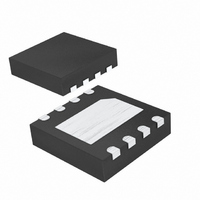
MAX7444ETA+T Maxim Integrated Products, MAX7444ETA+T Datasheet - Page 2

MAX7444ETA+T
Manufacturer Part Number
MAX7444ETA+T
Description
IC FILTER RECON VID 8-TDFN
Manufacturer
Maxim Integrated Products
Datasheet
1.MAX7443ESA.pdf
(8 pages)
Specifications of MAX7444ETA+T
Filter Type
Low Pass
Frequency - Cutoff Or Center
27MHz
Number Of Filters
2
Voltage - Supply
4.75 V ~ 5.25 V
Mounting Type
Surface Mount
Package / Case
8-TDFN Exposed Pad
Lead Free Status / RoHS Status
Lead free / RoHS Compliant
Max-order
-
ABSOLUTE MAXIMUM RATINGS
V
All Other Pins to GND.................................-0.3V to (V
Maximum Current into Any Pin Except V
Continuous Power Dissipation (T
Triple-Channel Video Reconstruction Filter and
Buffer for Composite and Y/C Outputs
ELECTRICAL CHARACTERISTICS
(V
T
Stresses beyond those listed under “Absolute Maximum Ratings” may cause permanent damage to the device. These are stress ratings only, and functional
operation of the device at these or any other conditions beyond those indicated in the operational sections of the specifications is not implied. Exposure to
absolute maximum rating conditions for extended periods may affect device reliability.
2
Passband Response
Stopband Attenuation
Boost Amplitude
Differential Gain
Differential Phase
Signal-to-Noise Ratio
Group Delay Deviation
Line-Time Distortion
Field-Time Distortion
Clamp Settling Time
Output DC Clamp Level
Low-Frequency Gain Accuracy
Group Delay Matching
Channel-to-Channel Crosstalk
Input Leakage Current
CC
A
CC
8-Pin Thin QFN (derate 24.4mW/°C above +70°C) ...1951mW
8-Pin SO (derate 18.9mW/°C above +70°C)..............1509mW
= T
_______________________________________________________________________________________
to GND ...........................................................................+6V
= +5V ±5%, C
MIN
to T
PARAMETER
MAX
, GSET = GND (6dB) and V
L
= 0 to 20pF, R
A
= +70°C)
t
SYMBOL
g(MATCH)
L
X
H
V
CC
SNR
A
dG
∆t
TALK
DIST
A
= 75Ω to GND for DC-couple, R
dθ
DIST
I
IN
SB
V
g
and GND .....±50mA
CC
(9.5dB), unless otherwise noted. Typical values are at T
f = 100kHz to 4.2MHz,
relative to 100kHz
f = 27MHz
f = 4.2MHz, MAX7444
5-step modulated
staircase
5-step modulated
staircase
Peak signal (2V
RMS noise, f = 100Hz to
50MHz
Deviation from 100kHz to
4.1MHz
18µs, 100 IRE bar
130 lines, 18µs, 100 IRE bar
To ±1%
YOUT
CVOUT
COUT
f = 100kHz, relative to 6dB
Low-frequency channel-to-channel matching,
f = 100kHz for YOUT and COUT
f = 100kHz to 3.58MHz, gain = 6dB
CC
+ 0.3V)
P-P
CONDITIONS
) to
Operating Temperature Range ...........................-40°C to +85°C
Storage Temperature Range .............................-65°C to +150°C
Junction Temperature ......................................................+150°C
Lead Temperature (soldering, 10s) .................................+300°C
L
= 75Ω to V
MAX7443
MAX7444
Gain = 6dB,
9.5dB, 12dB
Gain = 6dB,
9.5dB, 12dB
Gain = 6dB,
9.5dB, 12dB
MAX7443
MAX7444
CC
/2 for AC-couple, C
MIN
1.44
-0.8
-0.1
-3.5
0.6
0.6
39
67
A
= +25°C.)
+0.6
TYP
0.15
0.15
-0.3
430
0.6
0.8
0.8
1.6
41
73
12
61
8
2
YIN
+0.92
= C
MAX
+0.1
1.97
0.4
0.4
0.3
0.5
1.0
1.0
+2
20
30
10
CIN
Degrees
= 0.1µF,
UNITS
Lines
dB
dB
dB
dB
dB
µA
%
ns
%
%
%
ns
V


