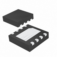
MAX7444ETA+T Maxim Integrated Products, MAX7444ETA+T Datasheet - Page 5

MAX7444ETA+T
Manufacturer Part Number
MAX7444ETA+T
Description
IC FILTER RECON VID 8-TDFN
Manufacturer
Maxim Integrated Products
Datasheet
1.MAX7443ESA.pdf
(8 pages)
Specifications of MAX7444ETA+T
Filter Type
Low Pass
Frequency - Cutoff Or Center
27MHz
Number Of Filters
2
Voltage - Supply
4.75 V ~ 5.25 V
Mounting Type
Surface Mount
Package / Case
8-TDFN Exposed Pad
Lead Free Status / RoHS Status
Lead free / RoHS Compliant
Max-order
-
Table 1. Gain-Setting Control
The GSET pin is biased internally to V
100kΩ resistors from V
ance at the node is 50kΩ. No additional connection is
necessary since the pin offers a minimum noise margin
immunity of 1V
When sync pulses in the luma signal (Y) are detected,
the DC restore loop is activated. The function of the
loop is to set the sync tip of the video signal to the
desired DC level of 0.8V for YOUT and COUT and the
average DC voltage of COUT at 1.6V.
Use a 0.1µF ceramic capacitor to AC-couple the input
to the MAX7443/MAX7444. This input capacitor stores
a DC level such that the outputs are clamped to the
appropriate DC voltage level.
The outputs of the MAX7443/MAX7444 are typically
connected to a 75Ω series back-match resistor fol-
lowed by the video cable. Because of the inherent
divide by two of this configuration, the blanking level of
the video cable is always less than 1V, which complies
with industry-standard video requirements. The video
buffer can also drive an AC-coupled video load. Good
video performance is achieved with an output capacitor
as low as 220µF.
The MAX7443/MAX7444 operate from a single +5V
supply. Bypass V
Place all external components as close to the device as
possible. Refer to the MAX7443 evaluation kit for a
proven PC board layout example.
Both the SO and thin QFN packages of the MAX7443/
MAX7444 have exposed pads on the bottom of the
packages. These pads are electrically connected to
GND and should be connected to the ground plane for
improved thermal conductivity. Do not route signals
under these packages.
_______________________________________________________________________________________________________
Triple-Channel Video Reconstruction Filter and
GSET
Open
GND
V
CC
Power-Supply Bypassing and Layout
P-P
Applications Information
.
CC
to GND with a 0.1µF capacitor.
CC
Buffer for Composite and Y/C Outputs
Output Considerations
to GND. The internal imped-
Input Considerations
Output Clamp Level
GAIN (dB)
9.5
12
12dB Gain Setting
6
Exposed Pads
CC
/2 through two
TRANSISTOR COUNT: 4252
PROCESS: BiCMOS
MAX7443ETA
MAX7443ESA
MAX7444ETA
MAX7444ESA
PART
TOP VIEW
GSET
GSET
GND
GND
CIN
YIN
CIN
YIN
1
2
4
1
2
4
3
3
THIN QFN
MAX7443
MAX7444
Pin Configurations
MAX7443
MAX7444
HIGH-FREQUENCY BOOST
SO
Chip Information
Selector Guide
7
6
5
7
6
5
8
8
Yes
Yes
No
No
YOUT
CVOUT
COUT
V
YOUT
CVOUT
COUT
V
CC
CC
5


