TDA5051AT/C1,512 NXP Semiconductors, TDA5051AT/C1,512 Datasheet - Page 6

TDA5051AT/C1,512
Manufacturer Part Number
TDA5051AT/C1,512
Description
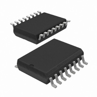
IC HOME AUTOMATION MODEM 16-SOIC
Manufacturer
NXP Semiconductors
Datasheet
1.TDA5051ATC1518.pdf
(29 pages)
Specifications of TDA5051AT/C1,512
Package / Case
16-SOIC (0.300", 7.5mm Width)
Data Format
ASK over Home Power Lines
Baud Rates
1.2k
Voltage - Supply
4.75 V ~ 5.25 V
Mounting Type
Surface Mount
Mounting Style
SMD/SMT
Lead Free Status / RoHS Status
Lead free / RoHS Compliant
Interface
-
Lead Free Status / Rohs Status
Lead free / RoHS Compliant
Other names
568-1136-5
935234750512
TDA5051ATD
935234750512
TDA5051ATD
Available stocks
Company
Part Number
Manufacturer
Quantity
Price
Company:
Part Number:
TDA5051AT/C1,512
Manufacturer:
Maxim
Quantity:
13
NXP Semiconductors
TDA5051A
Product data sheet
8.3.1 Transmission mode
8.3.2 Reception mode
8.2 Reception mode
8.3 Data format
8.4 Power-down mode
Remark: In transmission mode, the receiving part of the circuit is not disabled and the
detection of the transmitted signal is normally performed. In this mode, the gain chosen
before the beginning of the transmission is stored, and the AGC is internally set to
−6 dB as long as DATA_IN is LOW. Then, the old gain setting is automatically restored.
The input signal received by the modem is applied to a wide range input amplifier with
AGC (−6 dB to +30 dB). This is basically for noise performance improvement and signal
level adjustment, which ensures a maximum sensitivity of the ADC. An 8-bit conversion is
then performed, followed by digital band-pass filtering, to meet the CISPR16
normalization and to comply with some additional limitations met in current applications.
After digital demodulation, the baseband data signal is made available after pulse
shaping.
The signal pin (RX_IN) is a high-impedance input which has to be protected and
DC decoupled for the same reasons as with pin TX_OUT. The high sensitivity (82 dBμV)
of this input requires an efficient 50 Hz rejection filter (realized by the LC coupling
network), which also acts as an anti-aliasing filter for the internal digital processing;
(see
The data input (DATA_IN) is active LOW: this means that a burst is generated on the line
(pin TX_OUT) when DATA_IN pin is LOW.
Pin TX_OUT is in a high-impedance state as long as the device is not transmitting.
Successive logic 1s are treated in a Non-Return-to-Zero (NRZ) mode, see pulse shapes
in
The data output (pin DATA_OUT) is active LOW; this means that the data output is LOW
when a burst is received. Pin DATA_OUT remains LOW as long as a burst is received.
Power-down input (pin PD) is active HIGH; this means that the power consumption is
minimum when pin PD is HIGH. Now, all functions are disabled, except clock generation.
Figure 8
Figure
and
15).
All information provided in this document is subject to legal disclaimers.
Figure
Rev. 5 — 13 January 2011
9.
Home automation modem
TDA5051A
© NXP B.V. 2011. All rights reserved.
6 of 29


