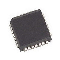
AMIS49587C5871RG ON Semiconductor, AMIS49587C5871RG Datasheet - Page 13

AMIS49587C5871RG
Manufacturer Part Number
AMIS49587C5871RG
Description
IC MODEM PLC 50/60MHZ 28PLCC
Manufacturer
ON Semiconductor
Specifications of AMIS49587C5871RG
Baud Rates
Selectable
Interface
SCI
Voltage - Supply
3 V ~ 3.6 V
Mounting Type
Surface Mount
Package / Case
28-PLCC
Number Of Transmitters
1
Power Supply Requirement
Single
Package Type
PLCC
Operating Temperature Classification
Commercial
Mounting
Surface Mount
Pin Count
28
Operating Temperature (max)
70C
Dual Supply Voltage (typ)
Not RequiredV
Dual Supply Voltage (max)
Not RequiredV
Dual Supply Voltage (min)
Not RequiredV
Lead Free Status / RoHS Status
Lead free / RoHS Compliant
Data Format
-
Lead Free Status / Rohs Status
Compliant
Available stocks
Company
Part Number
Manufacturer
Quantity
Price
Company:
Part Number:
AMIS49587C5871RG
Manufacturer:
ON
Quantity:
3 400
Company:
Part Number:
AMIS49587C5871RG
Manufacturer:
ON Semiconductor
Quantity:
10 000
4.1.4 Receiver External Parameters: Pin RX_IN, RX_OUT, REF_OUT
9. Input at RX_IN, no other external components.
10. Characterization data only. Not tested in production.
11. A sinusoidal signal of 10 kHz and 100 mVpp is injected between VDDA and VSSA. The signal level at the differential LPF_OUT and
12. A sinusoidal signal of 50 Hz and 100 mVpp is injected between VDDA and VSSA. The signal level at the differential LPF_OUT output is
13. These parameters will be tested in production with an input signal of 95 kHz and 1 Vp by reading out the digital samples at the point AD_OUT
The receive LPF filter + AGC + low noise amplifier must have a frequency characteristic between the limits listed below. The
absolute output level depends on the operating condition. In production the measurement will be done for relative output levels
where the 0 dB reference value is measured at 50 kHz with a signal amplitude of 100 mV.
Table 12. RECEIVER EXTERNAL PARAMETERS: Pin RX_IN, RX_OUT, REF_OUT
Input offset voltage 42 dB
Input offset voltage 0 dB
Max. peak input voltage
(corresponding to 62.5% of the SD
full scale)
Input referred noise of the analog
receiver path
Input leakage current of receiver
input
Max. current delivered by REF_OUT
Power supply rejection ratio of the
receiver input section
AGC gain step
AGC range
Analog ground reference output
voltage
Signal to noise ratio at 62.5% of the
SD full scale
Clipping level at the output of the
gain stage (RX_OUT)
Table 13. RECEIVER FREQUENCY CHARACTERISTICS
REF_OUT output is measured to determine the parameter.
measured to determine the parameter.
with the default settings of T_RX_MOD[7], SDMOD_TYP, DEC_TYP, and COR_F_ENA. The AGC gain is switched to 0 dB.
Frequency (kHz)
Parameter
1000
2000
130
165
330
660
10
95
AGC gain = 42 dB
AGC gain = 0 dB
AGC gain = 0 dB (Note 9)
AGC gain = 42 dB
(Notes 9 and 10)
AGC gain = 42 dB (Note 11)
AGC gain = 42 dB (Note 12)
(Notes 9 and 13)
Test Conditions
--0.5
--1.3
--4.5
Min
http://onsemi.com
Attenuation
13
PSRR
I
V
V
V
Max_REF_OUT
V
SN
CLIP_AGC_IN
V
OFFS_RX_IN
OFFS_RX_IN
AGC
I
MAX_RX_IN
NF
AGC
Symbol
LE_RX_IN
REF_OUT
AD_OUT
RX_IN
LPF_OUT
range
step
--18.0
--36.0
Max
--2.0
--3.0
--50
--55
0.5
0.5
--300
0.85
39.9
1.52
1.15
Min
5.7
--1
10
35
54
Typ
Unit
dB
dB
dB
dB
dB
dB
dB
dB
Max
1.15
44.1
1.78
1.65
150
300
6.3
50
5
1
nV/√Hz
Unit
mV
mV
mA
V
mA
dB
dB
dB
dB
Vp
V
p


