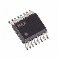
MXB7843EEE+ Maxim Integrated Products, MXB7843EEE+ Datasheet - Page 13

MXB7843EEE+
Manufacturer Part Number
MXB7843EEE+
Description
IC CNTRLR TOUCH RES 16QSOP
Manufacturer
Maxim Integrated Products
Type
Resistiver
Datasheet
1.MXB7843EEE.pdf
(21 pages)
Specifications of MXB7843EEE+
Touch Panel Interface
4-Wire
Number Of Inputs/keys
1 TSC
Resolution (bits)
12 b
Data Interface
MICROWIRE™, QSPI™, Serial, SPI™
Data Rate/sampling Rate (sps, Bps)
125k
Voltage Reference
External
Voltage - Supply
2.38 V ~ 5.25 V
Current - Supply
650µA
Operating Temperature
-40°C ~ 85°C
Mounting Type
Surface Mount
Package / Case
16-QSOP
Output Type
Digital
Interface
4-Wire Serial
Input Type
Analog
Maximum Operating Temperature
+ 85 C
Mounting Style
SMD/SMT
Minimum Operating Temperature
- 40 C
Lead Free Status / RoHS Status
Lead free / RoHS Compliant
The digital interface consists of three inputs, DIN, DCLK,
CS, and one output, DOUT. A logic-high on CS disables
the MXB7843 digital interface and places DOUT in a
high-impedance state. Pulling CS low enables the
MXB7843 digital interface.
Start a conversion by clocking a control byte into DIN
(Table 3) with CS low. Each rising edge on DCLK
clocks a bit from DIN into the MXB7843’s internal shift
register. After CS falls, the first arriving logic 1 bit
defines the control byte’s START bit. Until the START bit
arrives, any number of logic 0 bits can be clocked into
DIN with no effect.
The MXB7843 is compatible with SPI/QSPI/MICROWIRE
devices. For SPI, select the correct clock polarity and
sampling edge in the SPI control registers of the micro-
controller: set CPOL = 0 and CPHA = 0. MICROWIRE,
SPI, and QSPI all transmit a byte and receive a byte at
the same time. The simplest software interface requires
only three 8-bit transfers to perform a conversion (one 8-
bit transfer to configure the ADC, and two more 8-bit
transfers to read the conversion result) (Figure 7).
Make sure the CPU’s serial interface runs in master
mode so the CPU generates the serial clock. Choose a
clock frequency from 500kHz to 2MHz:
1) Set up the control byte and call it TB. TB should be
2) Use a general-purpose I/O line on the CPU to pull
3) Transmit TB and simultaneously receive a byte; call
4) Transmit a byte of all zeros ($00 hex) and simultane-
5) Transmit a byte of all zeros ($00 hex) and simultane-
6) Pull CS high.
Figure 7 shows the timing for this sequence. Bytes RB2
and RB3 contain the result of the conversion, padded
by four trailing zeros. The total conversion time is a func-
tion of the serial-clock frequency and the amount of idle
timing between 8-bit transfers.
in the format: 1XXXXXXX binary, where X denotes
the particular channel, selected conversion mode,
and power mode (Tables 3, 4).
CS low.
it RB1.
ously receive byte RB2.
ously receive byte RB3.
Initialization After Power-Up and Starting a
______________________________________________________________________________________
2.375V to 5.25V, 4-Wire Touch-Screen
Simple Software Interface
Digital Interface
Conversion
The MXB7843 outputs data in straight binary format
(Figure 10). Data is clocked out on the falling edge of
the DCLK, MSB first.
The external clock not only shifts data in and out, but it
also drives the analog-to-digital conversion steps.
BUSY pulses high for one clock period after the last bit
of the control byte. Successive-approximation bit deci-
sions are made and appear at DOUT on each of the
next 12 DCLK falling edges. BUSY and DOUT go into a
high-impedance state when CS goes high.
The conversion must complete in 500µs or less; if not,
droop on the sample-and-hold capacitors can degrade
conversion results.
The falling edge of CS does not start a conversion. The
first logic high clocked into DIN is interpreted as a start
bit and defines the first bit of the control byte. A conver-
sion starts on DCLK’s falling edge, after the eighth bit
of the control byte is clocked into DIN.
The first logic 1 clocked into DIN after bit 6 of a conver-
sion in progress is clocked onto the DOUT pin and is
treated as a START bit (Figure 8).
Once a start bit has been recognized, the current con-
version must be completed.
The fastest the MXB7843 can run with CS held continu-
ously low is 15 clock conversions. Figure 8 shows the
serial-interface timing necessary to perform a conver-
sion every 15 DCLK cycles. If CS is connected low and
DCLK is continuous, guarantee a start bit by first clock-
ing in 16 zeros.
Most microcontrollers (µCs) require that data transfers
occur in multiples of eight DCLK cycles; 16 clocks per
conversion is typically the fastest that a µC can drive the
MXB7843. Figure 9 shows the serial-interface timing nec-
essary to perform a conversion every 16 DCLK cycles.
The MXB7843 provides an 8-bit conversion mode
selected by setting the MODE bit in the control byte
high. In the 8-bit mode, conversions complete four
clock cycles earlier than in the 12-bit output mode,
resulting in 25% faster throughput. This can be used in
conjunction with serial interfaces that provide 12-bit
transfers, or two conversions could be accomplished
with three 8-bit transfers. Not only does this shorten each
conversion by 4 bits, but each conversion can also
Controller
8-Bit Conversion
Digital Output
Data Framing
Serial Clock
13


