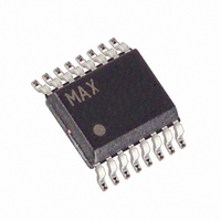
MXB7843EEE+ Maxim Integrated Products, MXB7843EEE+ Datasheet - Page 17

MXB7843EEE+
Manufacturer Part Number
MXB7843EEE+
Description
IC CNTRLR TOUCH RES 16QSOP
Manufacturer
Maxim Integrated Products
Type
Resistiver
Datasheet
1.MXB7843EEE.pdf
(21 pages)
Specifications of MXB7843EEE+
Touch Panel Interface
4-Wire
Number Of Inputs/keys
1 TSC
Resolution (bits)
12 b
Data Interface
MICROWIRE™, QSPI™, Serial, SPI™
Data Rate/sampling Rate (sps, Bps)
125k
Voltage Reference
External
Voltage - Supply
2.38 V ~ 5.25 V
Current - Supply
650µA
Operating Temperature
-40°C ~ 85°C
Mounting Type
Surface Mount
Package / Case
16-QSOP
Output Type
Digital
Interface
4-Wire Serial
Input Type
Analog
Maximum Operating Temperature
+ 85 C
Mounting Style
SMD/SMT
Minimum Operating Temperature
- 40 C
Lead Free Status / RoHS Status
Lead free / RoHS Compliant
the maximum rate during a conversion, conversions are
done less often. There is a significant difference in
power consumption between these two modes.
In this mode, the MXB7843 is powered down. This
mode becomes active after the current conversion
completes or on the next rising edge of CS, whichever
occurs first. The next command byte received on the
DIN returns the MXB7843 to full power. The first conver-
sion after the ADC returns to full power is valid.
This mode is reserved.
CS also places the MXB7843 into power-down. When
CS goes HIGH, the MXB7843 immediately powers
down and aborts the current conversion.
There are two key touch-screen characteristics that can
degrade accuracy. First, the parasitic capacitance
between the top and bottom layers of the touch screen
can result in electrical ringing. Second, vibration of the
top layer of the touch screen can cause mechanical
contact bouncing.
External filter capacitors may be required across the
touch screen to filter noise induced by the LCD panel
or backlight circuitry, etc. These capacitors lengthen
the settling time required when the panel is touched
and can result in a gain error, as the input signal may
not settle to its final steady-state value before the ADC
samples the inputs. Two methods to minimize or elimi-
nate this issue are described below.
One option is to lengthen the acquisition time by stopping
or slowing down DCLK, allowing for the required touch-
screen settling time. This method solves the settling time
problem for both single-ended and differential modes.
The second option is to operate the MXB7843 in the dif-
ferential mode only for the touch screen, and perform
additional conversions with the same address until the
input signal settles. The MXB7843 can then be placed
in the power-down state on the last measurement.
When using the MICROWIRE- (Figure 11) or SPI-com-
patible interface (Figure 12), set the CPOL = CPHA = 0.
Two consecutive 8-bit readings are necessary to obtain
the entire 12-bit result from the ADC. DOUT data transi-
tions occur on the serial clock’s falling edge and are
clocked into the µP on the DCLK’s rising edge. The first
Connection to Standard Interface
______________________________________________________________________________________
2.375V to 5.25V, 4-Wire Touch-Screen
Touch-Screen Settling
Hardware Power-Down
MICROWIRE Interface
PD1 = 0, PD0 = 1
PD1 = 1, PD0 = 0
8-bit data stream contains the first 8-bits of the current
conversion, starting with the MSB. The second 8-bit
data stream contains the remaining 4 result bits fol-
lowed by 4 trailing zeros. DOUT then goes high imped-
ance when CS goes high.
The MXB7843 can be used with the QSPI/SPI interface
using the circuit in Figure 12 with CPOL = 0 and CPHA
= 0. This interface can be programmed to do a conver-
sion on any analog input of the MXB7843.
Figure 13 shows an example circuit to interface the
MXB7843 to the TMS320. The timing diagram for this
interface circuit is shown in Figure 14.
Use the following steps to initiate a conversion in the
MXB7843 and to read the results:
1) The TMS320 should be configured with CLKX (trans-
For best performance, use printed circuit (PC) boards
with good layouts; wire-wrap boards are not recommend-
ed. Board layout should ensure that digital and analog
signal lines are separated from each other. Do not run
analog and digital (especially clock) lines parallel to one
another, or digital lines underneath the ADC package.
Establish a single-point analog ground (star ground
point) at GND. Connect all analog grounds to the star
2) The MXB7843’s CS pin is driven low by the
3) An 8-bit word (1XXXXXXX) should be written to the
4) The MXB7843’s BUSY output is monitored through
5) The TMS320 reads in 1 data bit on each of the next
6) Pull CS high to disable the MXB7843 until the next
mit clock) as an active-high output clock and CLKR
(TMS320 receive clock) as an active-high input
clock. CLKX and CLKR on the TMS320 are connect-
ed to the MXB7843 DCLK input.
TMS320’s XF I/O port to enable data to be clocked
into the MXB7843’s DIN pin.
MXB7843 to initiate a conversion and place the
device into normal operating mode. See Table 3 to
select the proper XXXXXXX bit values for your spe-
cific application.
the TMS320’s FSR input. A falling edge on the
BUSY output indicates that the conversion is in
progress and data is ready to be received from the
devices.
16 rising edges of DCLK. These bits represent the
12-bit conversion result followed by 4 trailing bits.
conversion is initiated.
Layout, Grounding, and Bypassing
Controller
TMS320LC3x Interface
QSPI/SPI Interface
17


