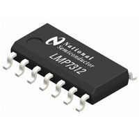
LMP7312MA/NOPB National Semiconductor, LMP7312MA/NOPB Datasheet - Page 2

LMP7312MA/NOPB
Manufacturer Part Number
LMP7312MA/NOPB
Description
IC AMP PROGRAM AFE 14SOIC
Manufacturer
National Semiconductor
Type
Programmable Amplifier/Attenuatorr
Datasheet
1.LMP7312MANOPB.pdf
(22 pages)
Specifications of LMP7312MA/NOPB
Input Type
Logic
Output Type
Logic
Interface
SPI
Current - Supply
2mA
Mounting Type
Surface Mount
Package / Case
14-SOIC (3.9mm Width), 14-SOL
Lead Free Status / RoHS Status
Lead free / RoHS Compliant
Other names
LMP7312MA
Available stocks
Company
Part Number
Manufacturer
Quantity
Price
Company:
Part Number:
LMP7312MA/NOPB
Manufacturer:
Intersil
Quantity:
840
www.national.com
Symbol
V
TCV
Av
e
I
I
R
R
CMRR
PSRR
ESD Rating
Analog Supply Voltage (V
DigitaI Supply Voltage (V
Attenuation pins -V
Amplification pins -IN, +IN referred to V
Voltage at all other pins referred to V
Storage Temperature Range
VA
VIO
n
OS
IN_CM
IN_DIFF
Absolute Maximum Ratings
If Military/Aerospace specified devices are required,
please contact the National Semiconductor Sales Office/
Distributors for availability and specifications.
5V Electrical Characteristics
Unless otherwise specified, all limits guaranteed for T
V
DE = Differential Output. Boldface limits apply at the temperature extremes.
Human Body Model
Machine Body Model
Charge device Model
CM_ATT
OS
=(+V
Core op-amp Input
Offset Voltage
Core op-amp Input
Offset Voltage
(Note
Gain Error
Gain Drift
Core op-amp Voltage
Noise Density
Core op-amp Peak to
Peak Voltage Noise
Analog Supply Current +V
Digital Supply Current Without any load connected to SDO pin
CM Input Resistance
Differential Input
Resistance
DC Common Mode
Rejection Ratio
Core op-amp DC
Power Supply
Rejection Ratio
(Note
IN
+(-V
Parameter
7)
2)
IN
, +V
IN
))/2, V
IN
DIO
S
= V
referred to V
=V
CM_AMP
+
IO
- V
-V
Nulling Switch Mode, DE, V
Nulling switch Mode, SE, -V
Nulling Switch Mode, DE, V
Nulling Switch Mode, SE, -V
Nulling Switch Mode, DE, V
Nulling Switch Mode, SE, -V
Nulling Switch Mode, DE, V
Nulling Switch Mode, SE, -V
All gains, R
SE / DE
RTI, Nulling Switch Mode, f = 10 kHz
RTI, Nulling Switch Mode, f= 0.1Hz to 10Hz
G= 0.192 V/V
G= 1 V/V
G= 0.192 V/V
G= 1 V/V
G= 0.096V/V, -15V < V
G= 0.192V/V, -11.4V < V
G= 0.384V/V, -6V < V
G= 0.768V/V, -3V < V
G= 1V/V, -2.3V < V
G= 2V/V, -1.15V < V
Nulling Switch Mode, 4.5V <V
-
-
)
=(+IN+(-IN))/2. Differential output configuration. SE = Single Ended Output,
)
-
IN
-
= −V
-
IN
L
= V
= 10 kΩ, C
-65°C to 150°C
(Note
OCM
(Note
Conditions
CM_AMP
CM_AMP
A
1)
CM_ATT
CM_ATT
±17.5V
= 25°C, V
2000V
1000V
CM_ATT
4)
L
150V
±10V
CM_ATT
= 50pF, SE / DE
6V
6V
6V
< 7.3V, SE / DE
OCM
OCM
OCM
OCM
OUT
< 6.15V, SE / DE.
OUT
OUT
OUT
< 11V, SE / DE
< 8V, SE / DE
+
< 15V, SE / DE
2
/V
<5.5V
/V
/V
/V
= 1V;
= 4V;
= 1V;
= 4V;
< 15V, SE / DE
+
R
For soldering specification:
Junction Temperature
= 5V, V
R
R
R
Analog Supply Voltage (V
=0V
Digital Supply Voltage (V
V
Attenuation pins -V
Amplification pins -IN, +IN referred to V
Temperature Range
Package Thermal Resistance
= 1V
Operating Ratings
= 4V
= 1V
= 4V
see product folder at www.national.com and
www.national.com/ms/MS/MS-SOLDERING.pdf
-
=0V
SOIC-14
IO
= 5V, V
−
= 0V, G = 0.192 V/V,
(Note
IN
–0.035
–0.045
–100
–250
–100
–250
, +V
(Note
Min
80
77
90
-3
-3
-5
IN
DIO
6)
S
3)
= V
referred to V
= V
(Note
(Note
+
IO
62.08
248.3
– V
±1.5
±1.5
7.25
Typ
160
±1
40
(Note
– V
3
-
3)
), V
5)
-
),
-
1)
-
-
(Note
0.035
0.045
Max
100
250
100
250
120
3
3
5
2
−40°C to 125°C
-2.35V to 7.35V
6)
4.5V to 5.5V
2.7V to 5.5V
-15V to 15V
145°C/W
ppm/°C
nV/
Units
µV/°C
µV
150°C
mA
kΩ
kΩ
µV
μA
dB
dB
%
PP


