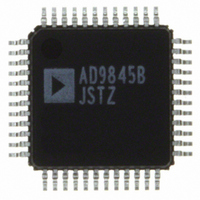
AD9845BJSTZ Analog Devices Inc, AD9845BJSTZ Datasheet - Page 3

AD9845BJSTZ
Manufacturer Part Number
AD9845BJSTZ
Description
IC CCD SIGNAL PROC 12BIT 48-LQFP
Manufacturer
Analog Devices Inc
Type
CCD Signal Processor, 12-Bitr
Datasheet
1.AD9845BJSTZRL.pdf
(24 pages)
Specifications of AD9845BJSTZ
Input Type
Logic
Output Type
Logic
Interface
3-Wire Serial
Mounting Type
Surface Mount
Package / Case
48-LQFP
Supply Voltage Range
2.7V To 3.6V
Ic Mounting
SMD
Tv / Video Case Style
LFCSP
No. Of Pins
48
Msl
MSL 3 - 168 Hours
Termination Type
SMD
Sample Rate
30MSPS
Data Interface
3-Wire, Serial
Filter Terminals
SMD
Rohs Compliant
Yes
Digital Ic Case Style
LQFP
Lead Free Status / RoHS Status
Lead free / RoHS Compliant
Current - Supply
-
Lead Free Status / RoHS Status
Lead free / RoHS Compliant, Lead free / RoHS Compliant
Available stocks
Company
Part Number
Manufacturer
Quantity
Price
Company:
Part Number:
AD9845BJSTZ
Manufacturer:
AD
Quantity:
560
Company:
Part Number:
AD9845BJSTZ
Manufacturer:
Analog Devices Inc
Quantity:
10 000
Company:
Part Number:
AD9845BJSTZRL
Manufacturer:
Analog Devices Inc
Quantity:
10 000
CCD MODE SPECIFICATIONS
Parameter
P
MAXIMUM CLOCK RATE
CDS
PIXEL GAIN AMPLIFIER (PxGA)
VARIABLE GAIN AMPLIFIER (VGA)
BLACK LEVEL CLAMP
SYSTEM PERFORMANCE
POWER-UP RECOVERY TIME
NOTES
1
2
Specifications subject to change without notice.
REV. B
RESET TRANSIENT
Input signal characteristics defined as follows:
PxGA gain fixed at Code 63 (3.3 dB).
OWER CONSUMPTION
Gain
Allowable CCD Reset Transient
Max Input Range before Saturation
Max CCD Black Pixel Amplitude
Max Input Range
Max Output Range
Gain Control Resolution
Gain Monotonicity
Gain Range (Twos Complement Coding)
Max Input Range
Max Output Range
Gain Control Resolution
Gain Monotonicity
Gain Range
Clamp Level Resolution
Clamp Level
Gain Accuracy
Peak Nonlinearity, 500 mV Input Signal
Total Output Noise
Power Supply Rejection (PSR)
Reference Standby Mode
Total Shutdown Mode
Power-Off Condition
500mV TYP
Min Gain (PxGA Gain Code 32)
Max Gain (PxGA Gain Code 31)
Low Gain (VGA Gain Code 77)
Max Gain (VGA Gain Code 1023)
Min Clamp Level
Max Clamp Level
Low Gain (VGA Code 77)
Max Gain (VGA Code 1023)
OPTICAL BLACK PIXEL
200mV MAX
2
INPUT SIGNAL RANGE
1V MAX
1
1
1
(T
MIN
Min
30
1.0
1.0
1.6
1.6
2.0
5.5
38.2
to T
Guaranteed
Guaranteed
MAX
Typ
153
0
500
200
64
–2.5
9.5
2
36
256
0
255
6
39.5
0.1
0.5
40
1
3
15
1024
, AVDD = DVDD = 3.0 V, f
Max
40.2
6.5
–3–
Unit
mW
MHz
dB
mV
V p-p
mV
V p-p
V p-p
Steps
dB
dB
V p-p
V p-p
Steps
dB
dB
Steps
LSB
LSB
dB
dB
%
LSB rms
dB
ms
ms
ms
DATACLK
= f
SHP
Notes
See TPC 1 for Power Curves
PxGA Gain at 4 dB
See Figure 28 for PxGA Gain Curve
See Figure 29 for VGA Gain Curve
Measured at ADC Output
Specifications Include Entire Signal Chain
Gain = (0.0353
12 dB Gain Applied
AC Grounded Input, 6 dB Gain Applied
Measured with Step Change on Supply
Normal Clock Signals Applied
= f
SHD
= 30 MHz, unless otherwise noted.)
Code) + 3.3
AD9845B


